
Method for monitoring matched machine overlay

a technology of overlay alignment and matching machine, which is applied in semiconductor/solid-state device testing/measurement, printing, instruments, etc., can solve the problem of uncertain relative accuracy of test results

Inactive Publication Date: 2005-10-18
MACRONIX INT CO LTD
View PDF14 Cites 10 Cited by
  • Summary
  • Abstract
  • Description
  • Claims
  • Application Information

AI Technical Summary

Benefits of technology

[0008]Therefore, there remains a need for a quick, efficient, and accurate method to evaluate overlay alignment.

Problems solved by technology

In addition, the relative accuracy of the Test is uncertain as the machine used to do the Test is itself used to manufacture the wafers.

Method used


Image

  • Method for monitoring matched machine overlay
  • Method for monitoring matched machine overlay

Examples


Embodiment Construction

[0001]1. Field of the Invention

[0002]This invention relates in general to a semiconductor manufacturing process and, more particularly, to a method for monitoring the accuracy of overlay alignment during photolithographic steps.

[0003]2. Background of the Invention

[0004]In semiconductor manufacturing process where a plurality of integrated circuits (“ICs”) are manufactured on a silicon wafer, a number of layers of semiconductor materials with various patterns of circuit layouts are overlaid on top of one another at predetermined locations. A machine known as a “stepper” is used at various stages of the manufacturing process to transfer circuit layout patterns onto a layer by exposing a photoresist to ultraviolet light through a mask, or reticle. The circuit layout pattern is transferred through the reticle onto a photoresist in a step and repeat manner. The reticle is moved at a predetermined distance at a time, and the photoresist is exposed to the pattern and developed. The movemen...


PUM


Abstract

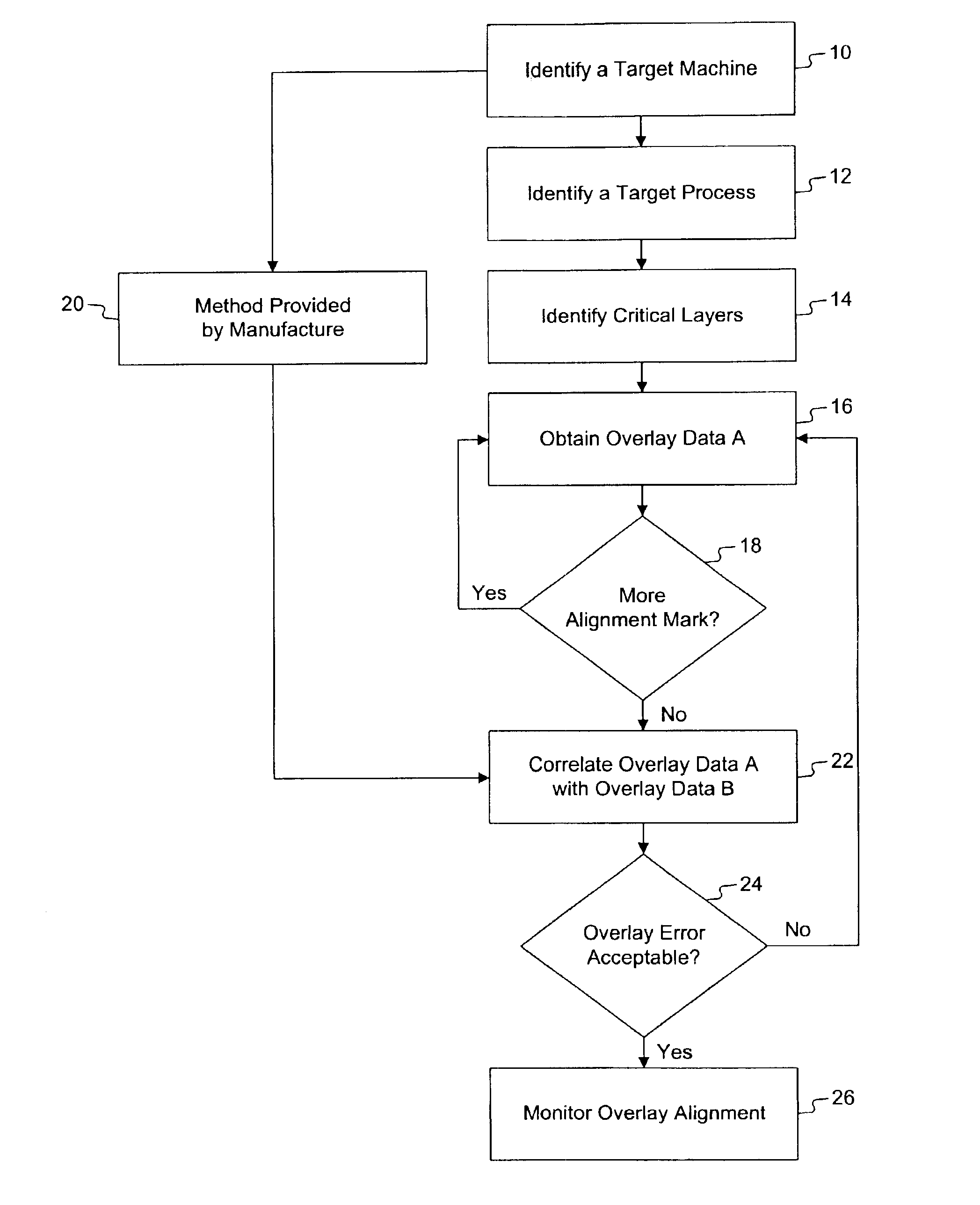
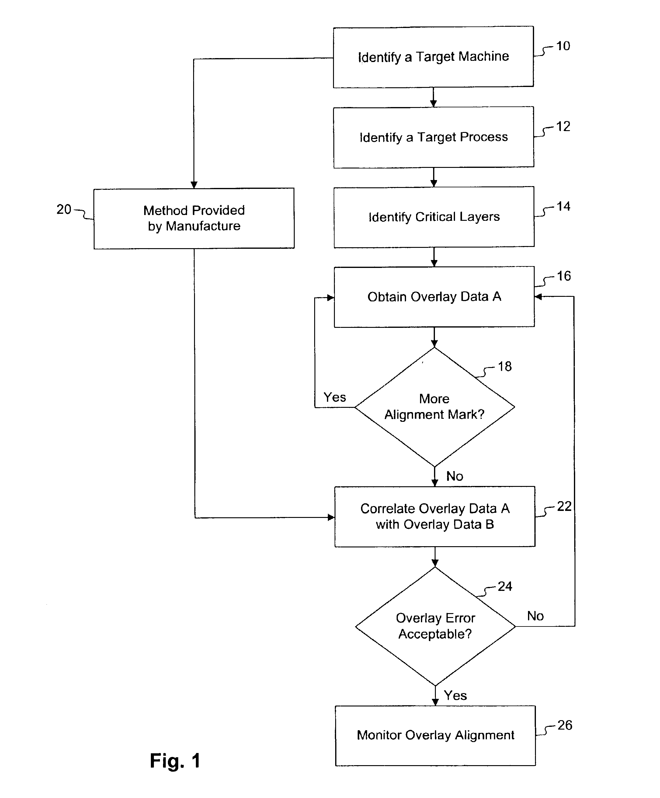
A method for monitoring overlay alignment on a wafer that includes identifying a target machine, identifying a target process, identifying a plurality of critical layers, obtaining a plurality of overlay data from at least one of designated registration patterns on the wafer as baseline data, providing a plurality of reference overlay data, correlating the plurality of the reference overlay data with the baseline data to obtain overlay error, comparing the overlay error with specifications of the target machine, accepting the baseline data when the overlay error is within the specifications, and performing overlay alignment monitoring with the baseline data.

Description

DESCRIPTION OF THE INVENTION[0001]1. Field of the Invention[0002]This invention relates in general to a semiconductor manufacturing process and, more particularly, to a method for monitoring the accuracy of overlay alignment during photolithographic steps.[0003]2. Background of the Invention[0004]In semiconductor manufacturing process where a plurality of integrated circuits (“ICs”) are manufactured on a silicon wafer, a number of layers of semiconductor materials with various patterns of circuit layouts are overlaid on top of one another at predetermined locations. A machine known as a “stepper” is used at various stages of the manufacturing process to transfer circuit layout patterns onto a layer by exposing a photoresist to ultraviolet light through a mask, or reticle. The circuit layout pattern is transferred through the reticle onto a photoresist in a step and repeat manner. The reticle is moved at a predetermined distance at a time, and the photoresist is exposed to the patter...

Claims


Application Information

Patent Timeline
IPC IPC(8): G03F9/00G06F17/50G06F19/00H01L21/66H01L21/02H01L21/027G03F7/20
CPCG03F7/70633
Inventor PENG, TSUNG-HANCHIEN, DING-CHIENLIU, CHUNG-HSINHSU, CHIH-CHIA
Owner MACRONIX INT CO LTD
Learn More