Method for manufacturing alignment mark of semiconductor device using STI process

Inactive Publication Date: 2005-10-25
SK HYNIX INC
View PDF9 Cites 11 Cited by
  • Summary
  • Abstract
  • Description
  • Claims
  • Application Information

AI Technical Summary

Benefits of technology

[0011]Accordingly, it is an object of the present invention to provide a method for manufacturing alignment mark of semiconductor device wherein a predetermined thickness of a device isolation film is etch

Problems solved by technology

Therefore, an accurate alignment in subsequent process using the

Method used


Image

  • Method for manufacturing alignment mark of semiconductor device using STI process
  • Method for manufacturing alignment mark of semiconductor device using STI process
  • Method for manufacturing alignment mark of semiconductor device using STI process

Examples


Example

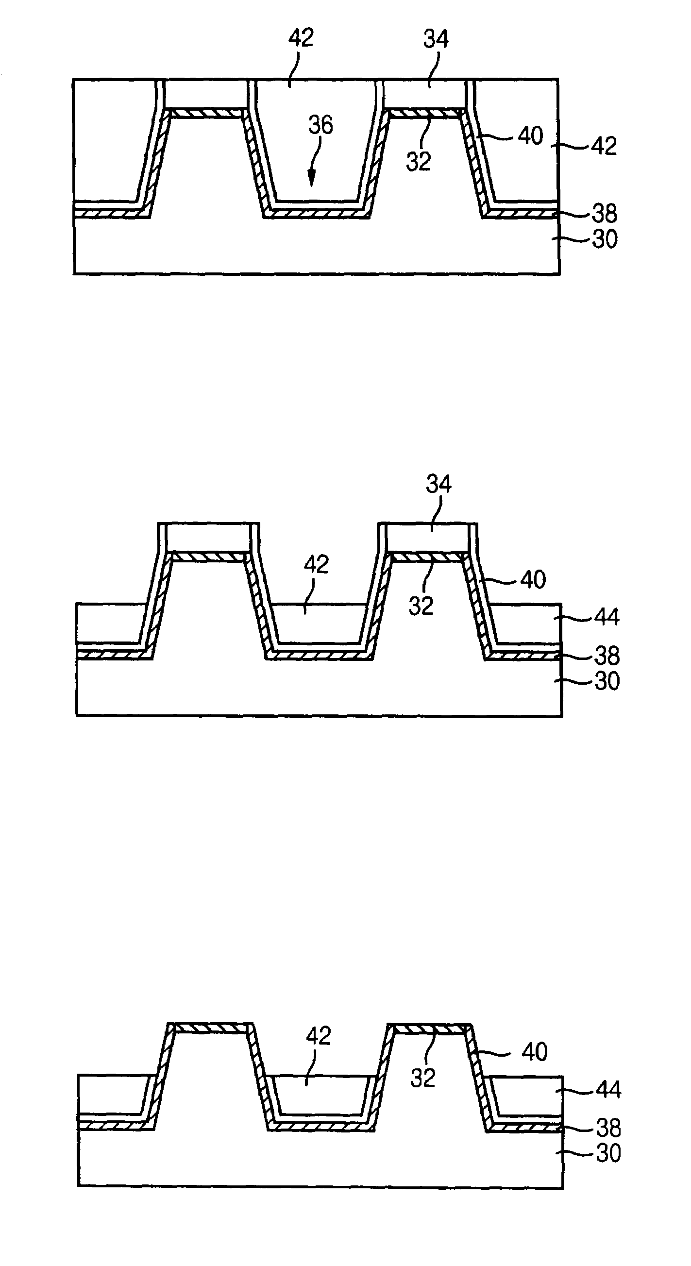
[0018]A method for manufacturing alignment mark of semiconductor device in accordance with a preferred embodiment of the present invention will now be described in detail with reference to the accompanying drawings.

[0019]FIGS. 4a through 4c are cross-sectional diagram illustrating a method for manufacturing alignment mark of semiconductor device in accordance with the present invention.

[0020]Referring to FIG. 4a, a pad oxide film (not shown) and a pad nitride film (not shown) are sequentially formed on a semiconductor substrate 30. The pad nitride film and the pad oxide film are etched via a photoetching process using a device isolation mask (not shown) to form a pad nitride film pattern 34 and a pad oxide film pattern 32. The semiconductor substrate 30 is then etched using the pad nitride film pattern 34 as a mask to form an alignment mark trench 36. Preferably, the alignment mark trench 36 has a depth ranging from 2000 to 10000 Å and the pad nitride film has a thickness ranging fr...


PUM


Abstract

The present invention discloses method for manufacturing alignment mark wherein a predetermined thickness of a device isolation film is etched prior to removing a pad nitride film during a shallow trench isolation process to increase contrast. In accordance with the method, a pad nitride film pattern and a pad oxide film pattern exposing a predetermined portion of the semiconductor substrate are formed. The semiconductor substrate is etched using the pad nitride film pattern as a mask to form an alignment mark trench. A device isolation film is formed in the trench and a predetermined thickness of the device isolation film is etched to form an alignment mark. The pad nitride film pattern is then removed.

Description

BACKGROUND OF THE INVENTION[0001]1. Field of the Invention[0002]The present invention relates to method for manufacturing alignment mark of semiconductor device, and in particular to an improved method for manufacturing alignment mark wherein a predetermined thickness of a device isolation film is etched prior to removing a pad nitride film during a STI (Shallow Trench Isolation) process to increase contrast for improving recognition capability of the alignment mark, thereby improving yield and reliability of semiconductor device.[0003]2. Description of the Background Art[0004]Generally, a semiconductor device comprises an active region where devices are formed and a device isolation region for defining the active region. In order to align masks accurately during subsequent processes, alignment marks are formed. One of the methods for forming alignment marks is by using STI trenches. That is, STI trenches filled with a device isolation film are formed and contrast generated due to a...

Claims


Application Information

Patent Timeline
IPC IPC(8): H01L21/70H01L21/762H01L23/544H01L21/027H01L21/76
CPCH01L21/76224H01L23/544H01L2223/54426H01L2223/54453H01L2924/0002H01L2924/00H01L21/76
Inventor KIM, HYUNG HWAN
Owner SK HYNIX INC
Why Eureka
Try Eureka