Method and apparatus for characterizing a circuit with multiple inputs

a circuit and input technology, applied in the field of circuit testing and measurement, can solve the problems of inability to allow inability to achieve independent measurement of pullup and pulldown performance, and significant complicating the design of such circuits

Inactive Publication Date: 2005-11-01
IBM CORP
View PDF3 Cites 29 Cited by
  • Summary
  • Abstract
  • Description
  • Claims
  • Application Information

AI Technical Summary

Problems solved by technology

Such measurements, however, do not allow the independent measurement of pullup and pulldown performance, but instead yield an average of the pullup and pulldown delays associated with the logic gates.
Furthermore, using conventional measurement methodologies, input and output slews are undesirably fixed by the condition that all gates drive and are driven by gates nominally identical to themselves.
This switching history dependence can significantly complicate the design of such circuits.
The presence of gate-to-body tunneling further complicates the device design.
Such experiments, however, have not agreed particularly well with model predictions.
More complex switching patterns in which the order of logic gate input switching varies over time, are not possible using conventional methodologies.

Method used


Image

  • Method and apparatus for characterizing a circuit with multiple inputs
  • Method and apparatus for characterizing a circuit with multiple inputs
  • Method and apparatus for characterizing a circuit with multiple inputs

Examples


Embodiment Construction

[0015]The present invention will be described herein with reference to circuits that are fabricated using a partially depleted silicon-on-insulator (SOI) process. As previously stated, modeling SOI devices and circuits is particularly difficult due, at least in part, to a body potential which may vary as a function of switching history. This body potential is created in part as a result of the floating body which is present in the SOI circuit. It is to be appreciated, however, that the techniques of the present invention are not limited to SOI circuits. Rather, the techniques of the invention may be similarly used to more accurately model and characterize devices and circuits formed using alternative fabrication processes, such as, but not limited to, a conventional bulk CMOS process.

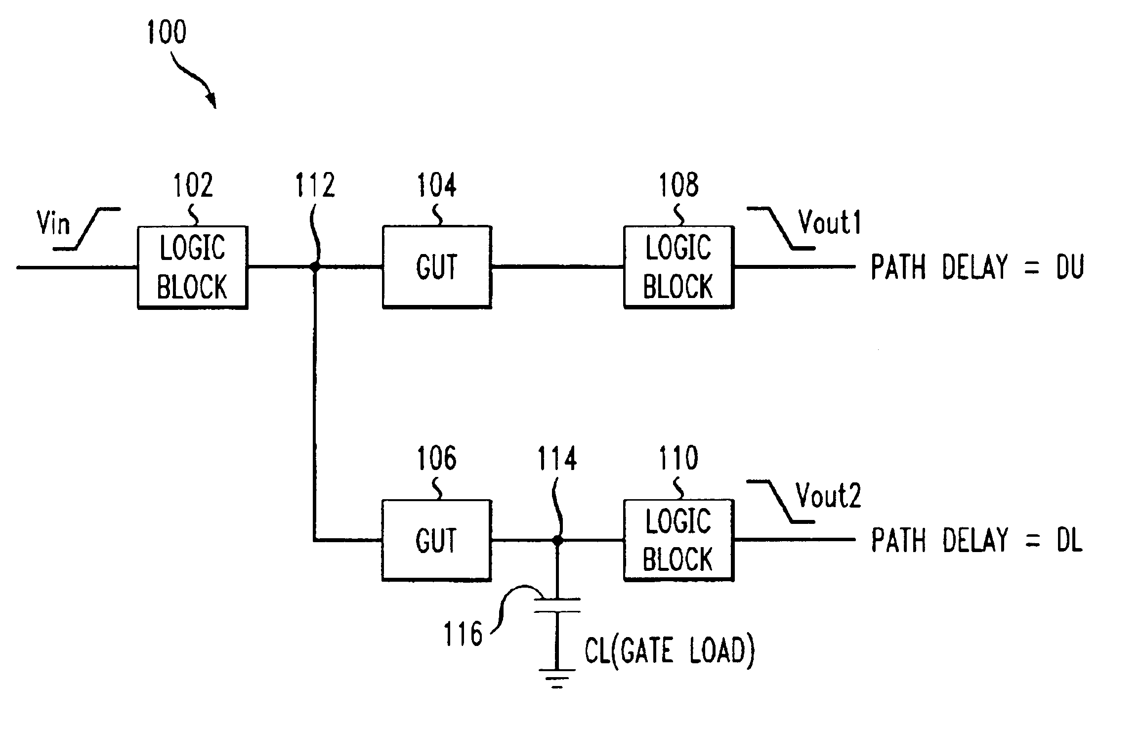
[0016]FIG. 1 shows an exemplary characterization circuit 100 illustrating the methodologies of the present invention. As apparent from the figure, an input signal Vin, which may be generated from an ext...


PUM


Abstract

A method of characterizing a circuit comprises the steps of measuring a first delay associated with the circuit when the circuit is substantially unloaded; measuring a second delay associated with the circuit when the circuit is loaded by a predetermined impedance; determining a difference between the second delay and the first delay, the delay difference corresponding to a switching impedance associated with the circuit; and determining a characterization parameter of the circuit, the characterization parameter being a function of at least the switching impedance associated with the circuit. The methodologies of the present invention are directed primarily to individually evaluating pullup and pulldown delays with substantial precision (e.g., sub-picosecond) for a representative set of circuits in the presence of an arbitrary switching history.

Description

FIELD OF THE INVENTION[0001]The present invention relates generally to test and measurement of devices and circuits, and more particularly relates to techniques for characterizing a circuit having multiple inputs.BACKGROUND OF THE INVENTION[0002]The high speed performance of a digital logic gate is commonly characterized using circuits such as ring oscillators, delay chains and the like. In these circuits, the time T for a signal to propagate through some number n of identical gates is measured and the delay per stage is typically determined as T / n. Such measurements, however, do not allow the independent measurement of pullup and pulldown performance, but instead yield an average of the pullup and pulldown delays associated with the logic gates. Furthermore, using conventional measurement methodologies, input and output slews are undesirably fixed by the condition that all gates drive and are driven by gates nominally identical to themselves. Each gate generally has a single input ...

Claims


Application Information

Patent Timeline
Patent Type & Authority Patents(United States)
IPC IPC(8): G01R31/30G01R31/28
CPCG01R31/3016
Inventor ANDERSON, CARL J.BHUSHAN, MANJULKETCHEN, MARK B.
Owner IBM CORP
Why Eureka
Try Eureka