High density chip carrier with integrated passive devices

a chip carrier and passive device technology, applied in the field of high density chip carrier with integrated passive device, can solve the problems of increasing the number of switching events, exacerbate the problem, and the parasitic inductance of the currently used discrete capacitor is not sufficiently low to be used, and achieves low inductance, low resistance integration, and fast electrical access

Inactive Publication Date: 2005-11-08
GLOBALFOUNDRIES U S INC
View PDF6 Cites 357 Cited by
  • Summary
  • Abstract
  • Description
  • Claims
  • Application Information

AI Technical Summary

Benefits of technology

[0009]The present invention pertains to the design, fabrication, and the resulting structures that enable integration of passive circuit elements, such as capacitors and resistors, within a close proximity of the relevant circuit elements on a chip. More specifically it overcomes the difficulties associated with the slower access times of discrete passives mounted on the microelectronic chip packages. The invention provides a low inductance and low resistance integration of active circuit elements with passive elements. In particular, it is an object of this invention to provide a structure for an integrated carrier which includes passive elements for high frequency and high speed computing applications. It is further an object of this invention to combine capacitors and / or resistors to form a complete high density interconnect structure with integrated passive devices within a silicon-based chip carrier. It is further an object of this invention to enable fast electrical access between the circuits on the chip and the passives on the carrier by virtue of low inductance input / output means such as area array solder bumps.

Problems solved by technology

The increase in power efficiency required in microprocessor units, especially for portable computing and communication needs, has further exacerbated the problem.
A proposed solution is clock gating (the ability to turn off clock circuits in unused parts of the chip); however, this increases the number of switching events dramatically and brings new complications because of greatly increased I noise.
In the case of electronic package applications, currently used discrete capacitors do not have sufficiently low enough parasitic inductance to be used in the high frequency or high speed circuits being proposed for the near future.

Method used


Image

  • High density chip carrier with integrated passive devices
  • High density chip carrier with integrated passive devices
  • High density chip carrier with integrated passive devices

Examples


first embodiment

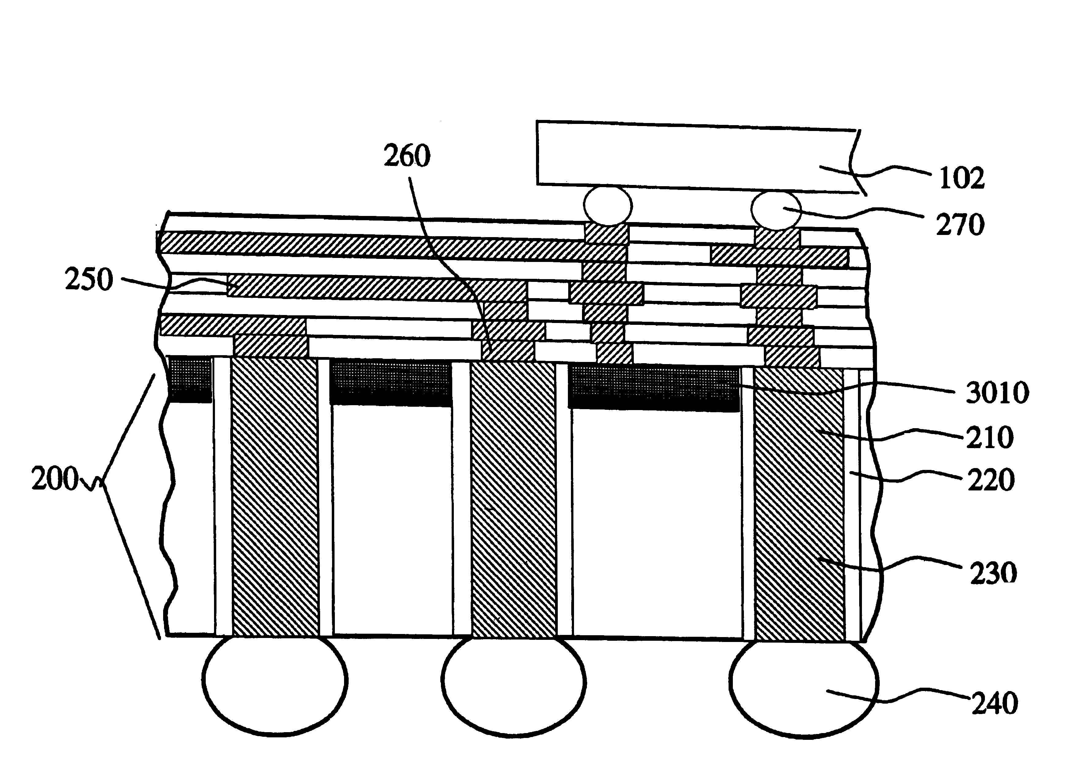
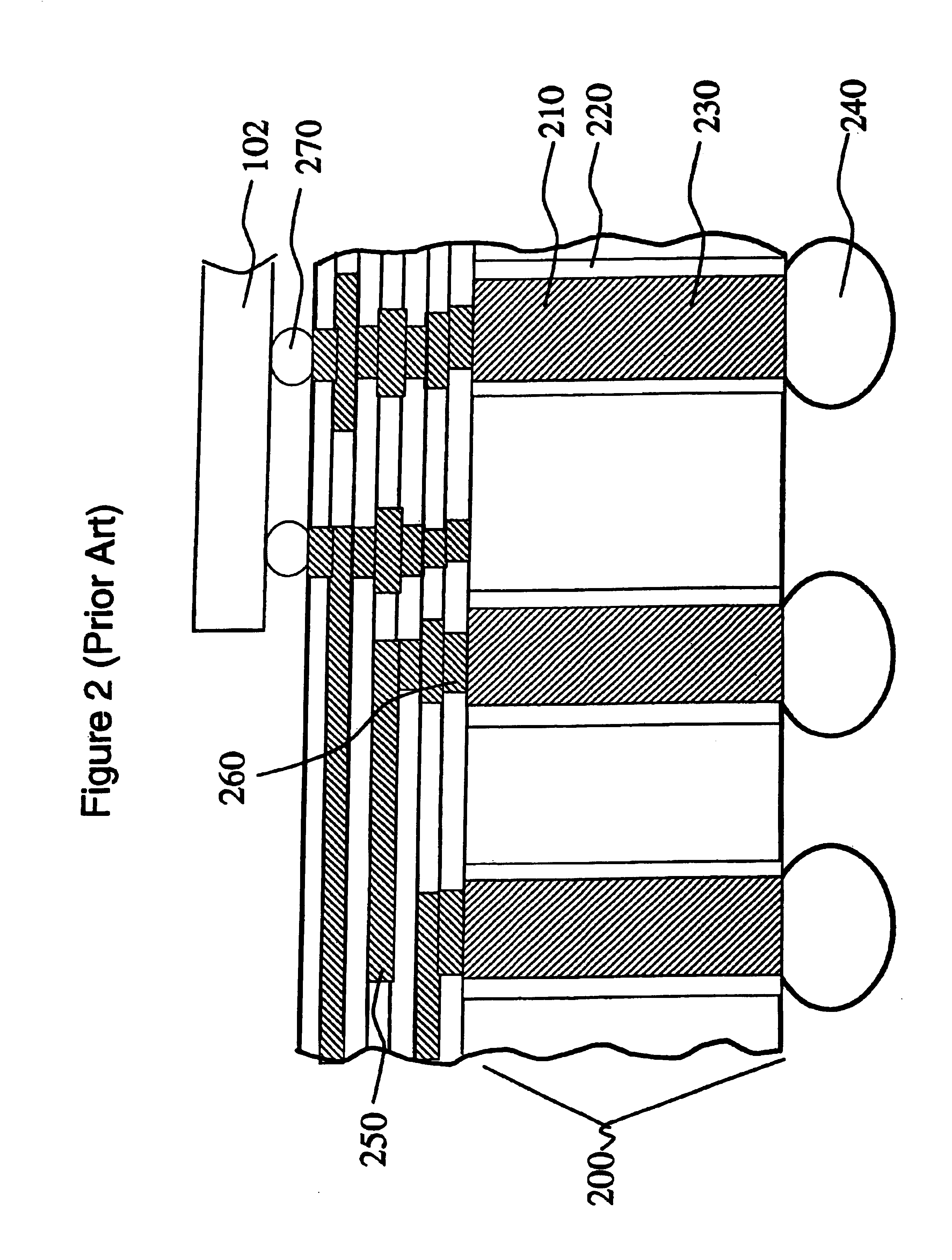
[0030]our inventive design enhances the prior art silicon carrier by adding integrated decoupling capacitors and allowing these passive elements to be accessed by the chips mounted on the carrier through the micro joint I / O connections. The decoupling capacitor arrays in the form of deep trench capacitors are built on the top surface region of the silicon carrier which is not already occupied by the through via features. FIG. 3a shows the schematic representation of such a structure. This embodiment comprises all the prior art features depicted in FIG. 2, but additionally comprises deep trench decoupling capacitor structures 3010 formed adjacent to the silicon through vias 210. State of the art processing used in the fabrication of these deep trenches 3010, such as lithography and reactive ion etching, allows for up to 40:1 aspect ratio, which means that trenches are 40 times as deep as they are wide. The trenches used in the process of this invention have widths between 100 nm and ...

second embodiment

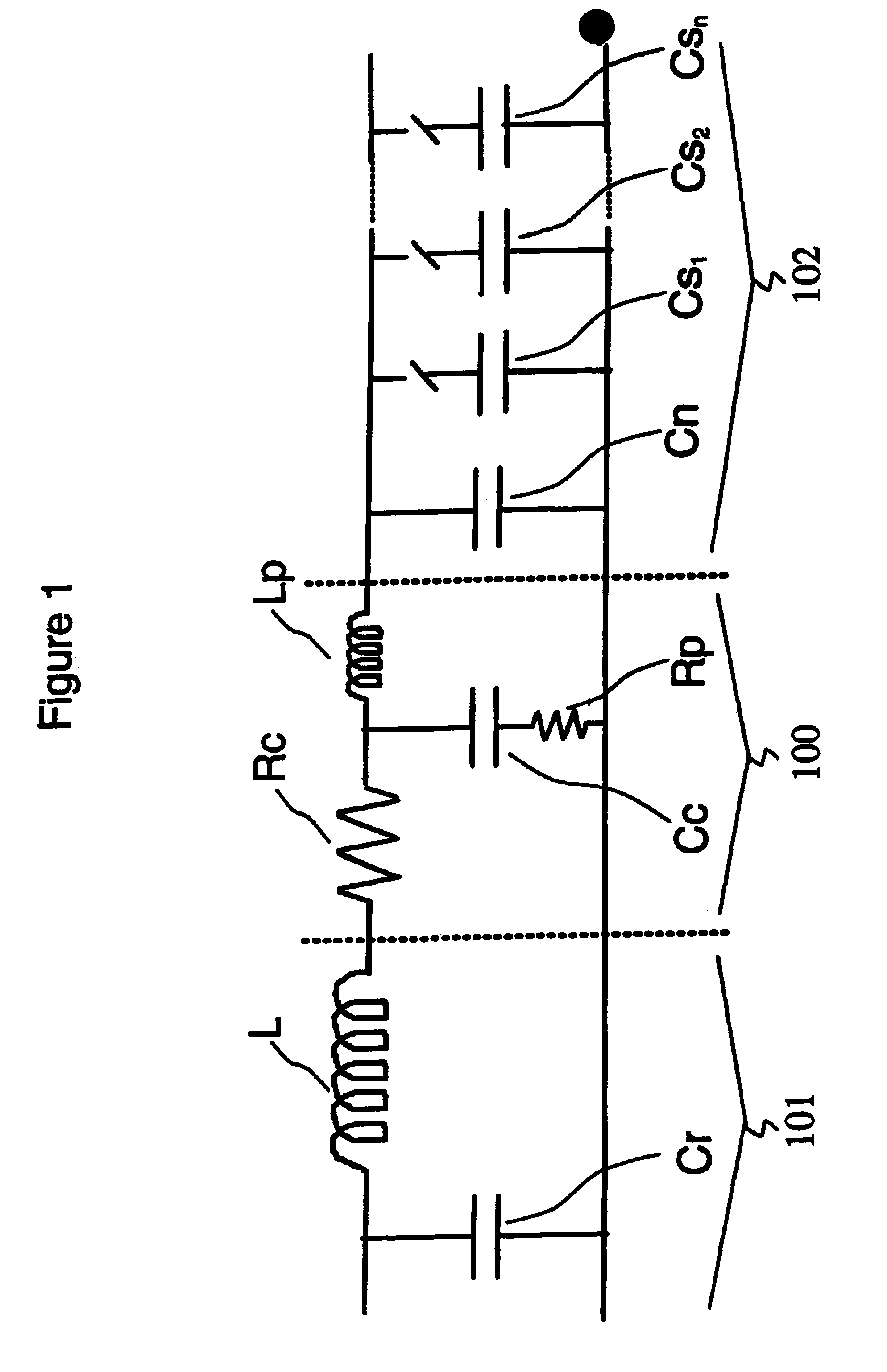
[0033]In a second embodiment, the second trench capacitor option designated as metal-insulator-silicon (MIS) depicted schematically in FIG. 3c is used. As in the case of the MIM option of FIG. 3b, the MIS trench capacitors of FIG. 3c are also situated on the top surface of the silicon carrier in the spaces between the through vias. In the MIS option, after the trenches 3010 are formed, an implantation and anneal step is performed to render the trench surfaces and tops highly conductive creating a heavily doped “well” region 3080′. This well 3080′ acts as the bottom electrode in this structure. The dopants are implanted with a doping concentration in the range of 10−18 to 10−21 atoms / cm2 to achieve low resistivity (<0.01 ohm-cm). The depth of the doping region may vary in the range of 50 nm to 500 nm. Dopants that can be used in forming the bottom conductive layer may be As, P, B and combinations thereof.

[0034]The rest of the process flow is identical to the MIM process flow except a...


PUM


Abstract

A carrier for a semiconductor component is provided having passive components integrated in its substrate. The passive components include decoupling components, such as capacitors and resistors. A set of connections is integrated to provide a close electrical proximity to the supported components.

Description

CROSS-REFERENCE TO RELATED APPLICATIONS[0001]This application is a continuation of and claims priority from U.S. patent application Ser. No. 10 / 314,589, filed on Dec. 9, 2002.BACKGROUND OF THE INVENTION[0002]1. Field of the Invention[0003]The present invention relates to the integration of passive elements into a silicon carrier structure for connecting integrated circuits, components, and other semiconductor components.[0004]2. Brief Description of Related Developments[0005]In advanced electronic computing systems the decoupling capacitors serve as a charge reservoir to support instantaneous current surges that invariably accompany simultaneous circuit switching. They are employed on chip and across all levels of packaging, including single chip and multi chip modules, board and back plane. In addition these passive components are required in the power distribution systems for integrated circuits (IC) to reduce the simultaneous circuit switching noise, or ΔI (Delta I) noise. Howeve...

Claims


Application Information

Patent Timeline
Patent Type & Authority Patents(United States)
IPC IPC(8): H01L23/48H01L23/50H05K1/16H05K3/46H01L23/12H01L25/04H01L25/18H01L29/40
CPCH01L23/50H01L23/49827H05K1/162H01L23/147H01L23/481H01L2924/01078H01L2924/15311H01L2924/157H01L2924/30105H05K1/167H05K3/4602H05K2201/09809H01L2924/01019H01L2924/01055H01L2224/16225H01L2924/01077H01L29/40
Inventor CHUDZIK, MICHAEL PATRICKDENNARD, ROBERT H.DIVAKARUNI, RAMAFURMAN, BRUCE KENNETHJAMMY, RAJARAONARAYAN, CHANDRASEKHARPURUSHOTHAMAN, SAMPATHSHEPARD, JR., JOSEPH F.TOPOL, ANNA WANDA
Owner GLOBALFOUNDRIES U S INC
Why Eureka
Try Eureka