Programmable logic device with redundant circuitry

a logic device and circuit technology, applied in logic circuits using specific components, instruments, pulse techniques, etc., can solve problems such as architecture that presented particular challenges in implementing redundancy

Inactive Publication Date: 2005-11-15
ALTERA CORP
View PDF13 Cites 48 Cited by
  • Summary
  • Abstract
  • Description
  • Claims
  • Application Information

AI Technical Summary

Benefits of technology

[0009]In some embodiments, the present invention provides a programmable logic device including redundant circuitry for connections between logic region rows and signal paths spanning a plurality of logic regions rows, the signal paths each including respective pluralities of lines. In some embodiments, redundant circuitry is provided for connections between logic region rows and respective lines spanning respective pluralities of logic region rows where the respective lines span fewer rows than are included in a defined repairable region above a spare row. In some embodiments, normal and redundant stitching circuitry provide routing and redundant routing over signal paths including respective pluralities of lines. In some particular embodiments, a stitching multiplexor of a first signal path is used for redundant routing by a second signal path and normal mode connections for one logic region row to drive the second signal path through the stitching multiplexor may overlap with redundant mode connections to drive the first signal path through the stitching multiplexor. In some embodiments, both upstream and downstream signal paths having pluralities of lines are provided with redundancy on either the same or different track bundles. In some particular embodiments, tracks of physical lines and associated stitching and redundant stitching circuitry provide signal paths that may stitch from one track to another in certain rows. In some embodiments, stubs provide pathways between lines and routing resources of a logic region row and between lines and stitching circuitry. In certain embodiments, the present invention provides redundancy for IO bus signal paths where the signal paths include respective pluralities of lines. In one embodiment, IO circuitry is provided to listen to a particular IO bus signal path over the same IO buffer in a majority of rows even as the IO bus signal path is provided on different physical lines over the length of the signal path. In some embodiments, dedicated routing between logic regions in different rows is provided with circuitry to accomplish bypassing rows as needed in normal and redundant modes.

Problems solved by technology

Such a routing architecture presented particular challenges to implementing redundancy.

Method used


Image

  • Programmable logic device with redundant circuitry
  • Programmable logic device with redundant circuitry
  • Programmable logic device with redundant circuitry

Examples


Embodiment Construction

[0034]The following description is presented to enable any person skilled in the art to make and use the invention, and is provided in the context of particular applications and their requirements. Various modifications to the disclosed embodiments will be readily apparent to those skilled in the art, and the generic principles defined herein may be applied to other embodiments and applications without departing from the spirit and scope of the invention. Thus, the present invention is not intended to be limited to the embodiments shown, which are merely descriptive of several specific embodiments illustrating the principles and features of the present invention.

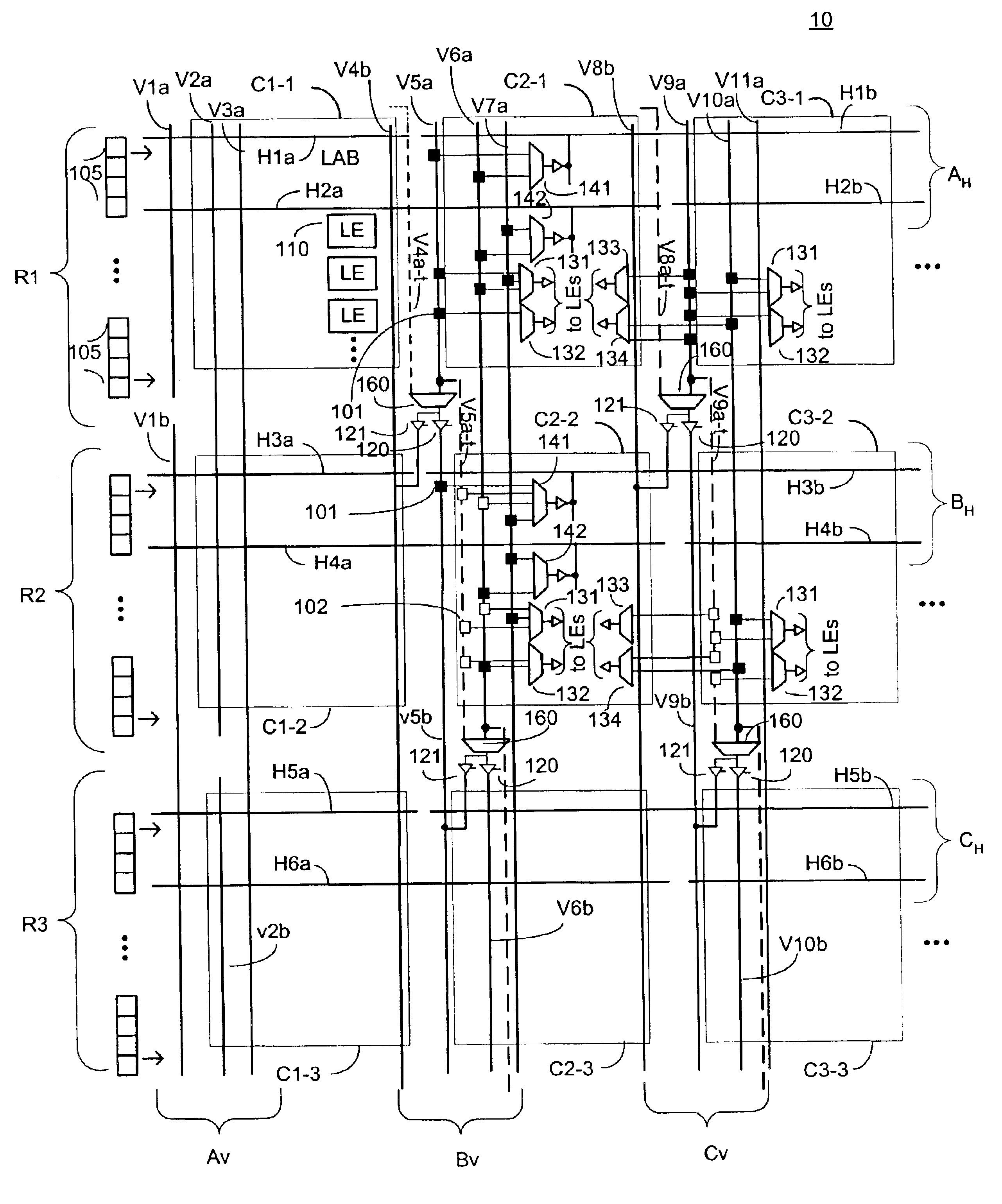
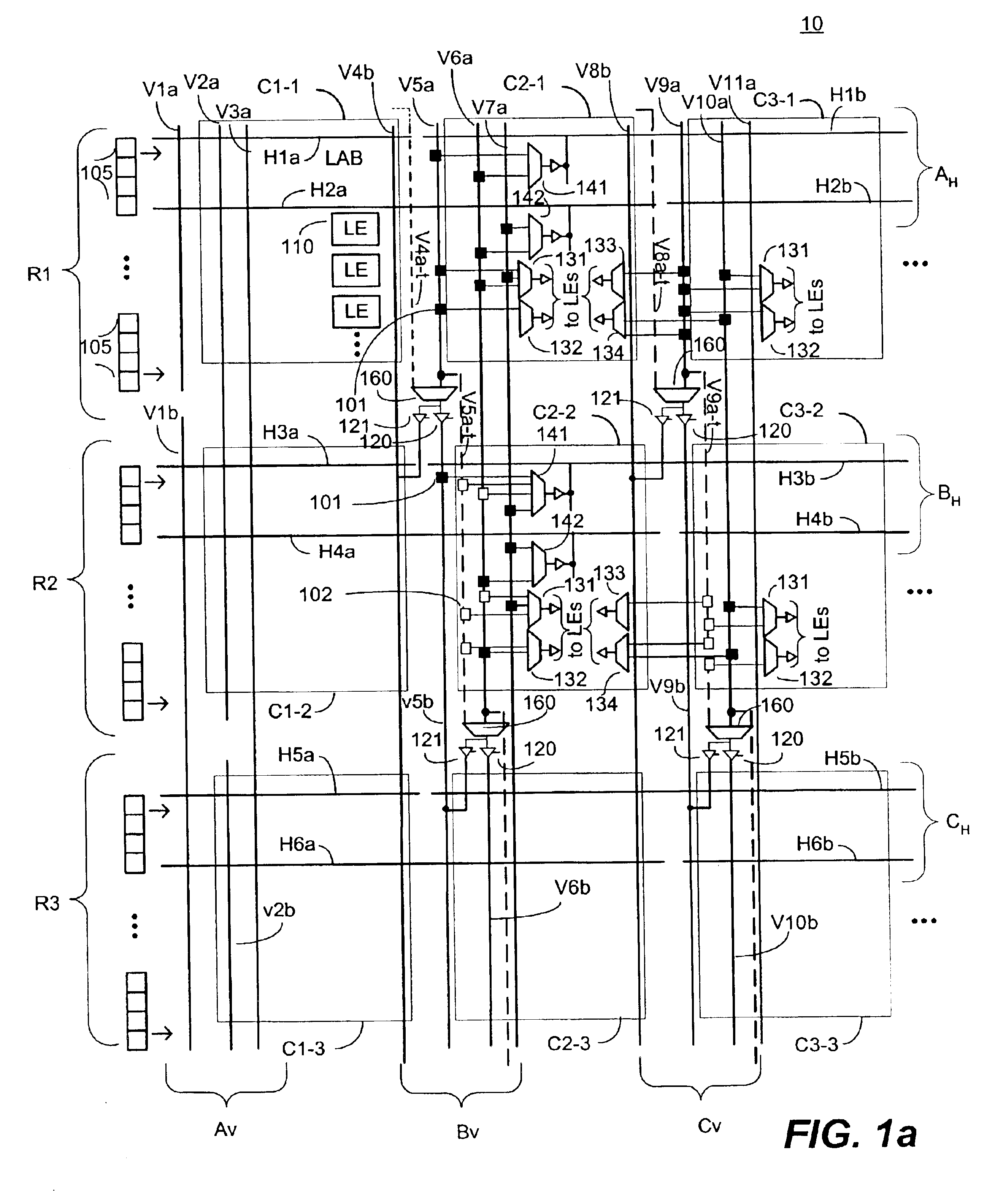
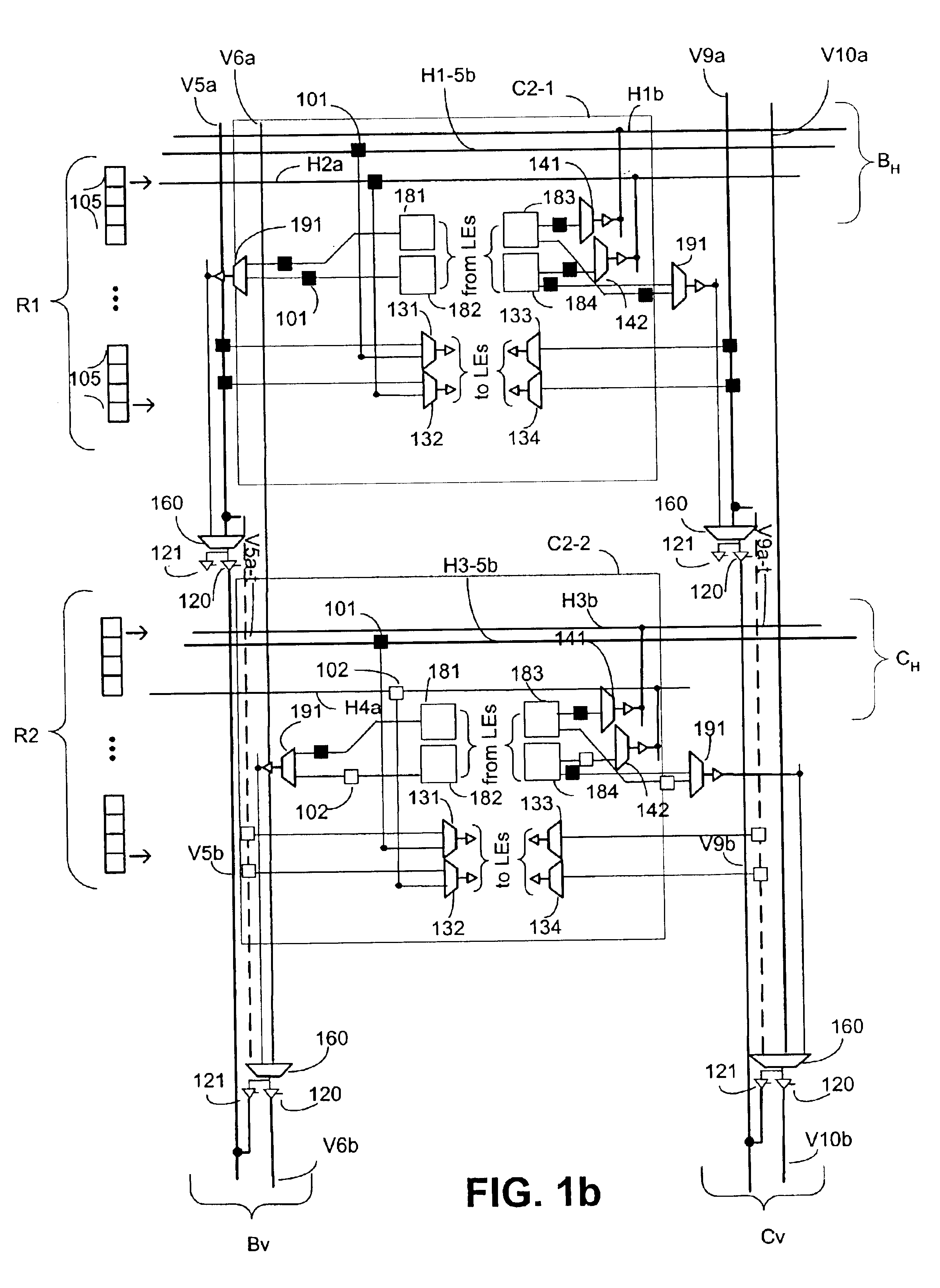
[0035]FIG. 1a illustrates a PLD section IO of a programmable logic device. PLD section 10 includes logic regions comprising logic array blocks (LABs) C1-1, C2-1, C3-1, C1-2, C2-2, C3-2, C1-3, C2-3, and C3-3. Each LAB in section 10 has logic elements (LEs) 110. Some LEs 110 are shown individually for LAB C1-1, but are not sho...


PUM


Abstract

A programmable logic device and associated method is provided with repairable regions. In one aspect, general routing interconnect lines are segmented within repairable regions. In another aspect, IO bus lines and associated circuitry are provided that accommodate redundancy in a staggered segmented architecture. In another aspect, a dedicated routing architecture between particular logic regions accommodates shifting to define and utilize repairable regions. Principles of other aspects are illustrated and described in the context of several exemplary embodiments of aspects of the invention.

Description

TECHNICAL FIELD[0001]This invention relates to programmable logic devices having redundant circuitry.BACKGROUND OF THE INVENTION AND RELATED ART[0002]Programmable logic devices (“PLDs”) (also sometimes referred to as PALs, PLAs, FPLAs, EPLDs, EEPLDs, LCAs, or FPGAs), are well-known integrated circuits that provide the advantages of fixed integrated circuits with the flexibility of custom integrated circuits. Such devices are well known in the art and typically provide an “off the shelf” device having at least a portion that can be electrically programmed to meet a user's specific needs. Application specific integrated circuits (“ASICs”) have traditionally been fixed integrated circuits; however, it is possible to provide an ASIC that has a portion or portions that are programmable; thus, it is possible for an integrated circuit device to have qualities of both an ASIC and a PLD. The term PLD as used herein will be considered broad enough to not necessarily exclude such devices.[0003...

Claims


Application Information

Patent Timeline
Patent Type & Authority Patents(United States)
IPC IPC(8): H03K19/177H01L21/82
CPCH03K19/17736H03K19/17744H03K19/17764
Inventor LANE, CHRISTOPHERZAVERI, KETANYI, HYUNPOWELL, GILESLEVENTIS, PAULJEFFERSON, DAVIDLEWIS, DAVIDNGUYEN, TRIETSANTURKAR, VIKRAMCHAN, MICHAELLEE, ANDYJOHNSON, BRIANCASHMAN, DAVID
Owner ALTERA CORP
Why Eureka
Try Eureka