Tape-packaged headed pin contact

a head pin and tape-packing technology, applied in the field of electronic industry, can solve the problems of pin damage, and requiring specialized equipment and packaging

Inactive Publication Date: 2005-11-22
AUTOSPLICE SYST
View PDF10 Cites 4 Cited by
  • Summary
  • Abstract
  • Description
  • Claims
  • Application Information

AI Technical Summary

Benefits of technology

[0010]Another object of the invention is a novel male electrically-conductive contact member that can be reliably solder-attached to a through-hole in a thin or soft-material substrate without using an interference fit.
[0012]These and other objects are achieved in accordance with one feature of the invention by a novel electrically-conductive contact member, characterized by a shank sized for a loose fit in a substrate through-hole and topped by a head whose diameter exceeds that of the through-hole. The head can be used by an industry standard pick-up nozzle of standard SMT placement equipment to conveniently drop the contact member into the board through-hole, with the head resting on the substrate surface.

Problems solved by technology

A problem with this approach is that it requires specialized insertion equipment and component packaging and processing.
Also, pin interference can cause damage to the pins.2. Surface Mount in Paste: In a conventional purely “top side”, non-through hole application, solder paste is applied to a surface mount pad and a pin is placed onto the pad.
The same problem with this approach exists, namely, it requires specialized equipment and packaging, and provides a single-sided pin interconnect only.3. Compliant Pins: In this application, no solder is required and a spring-like interference fit is used to make contact to a plated through-hole in the PCB.
Again, this approach requires specialized equipment and packaging.
These standard approaches will not satisfy the requirements for a reliable soldered pin interconnect where very thin boards are used, or where an intrusive interference lit or second-sided surface mount processing can not be used.
Also, softer materials such as Teflon can not withstand the forces needed with interference pins to retain the pin into the plated through-hole of the bare board accurately.
Still further, there are times when board hole diameter tolerances cannot be held tight enough for an interference fit with smaller pins.

Method used


Image

  • Tape-packaged headed pin contact
  • Tape-packaged headed pin contact
  • Tape-packaged headed pin contact

Examples


Embodiment Construction

[0025]The contact member of the invention can be fabricated with different cross-sections, such as round, square, rectangular, and octagonal, etc.

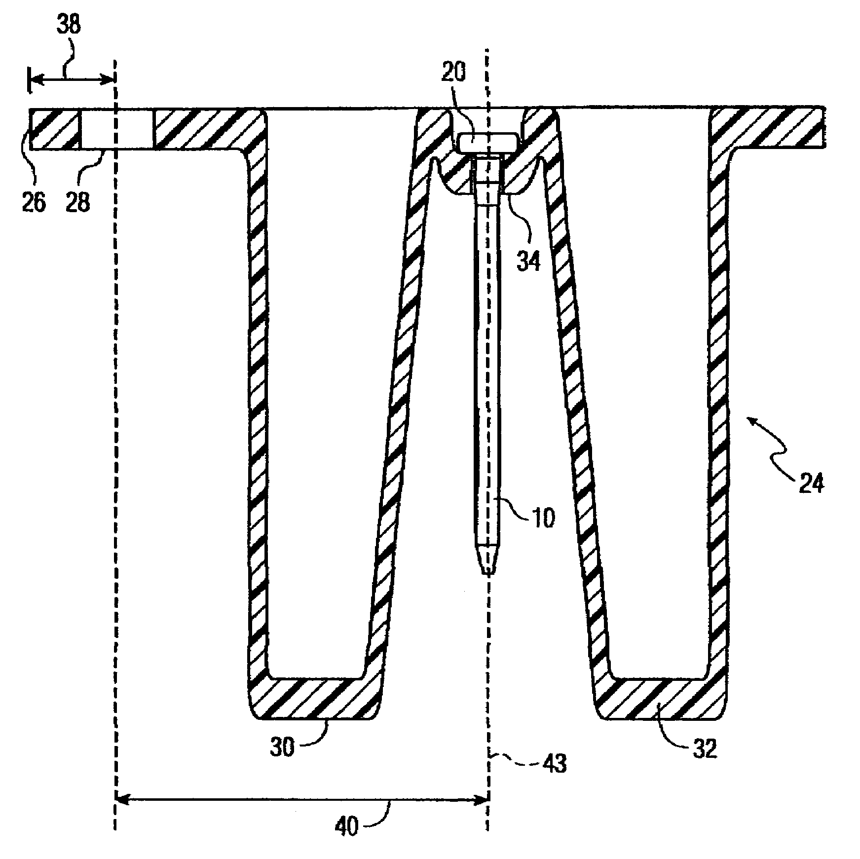
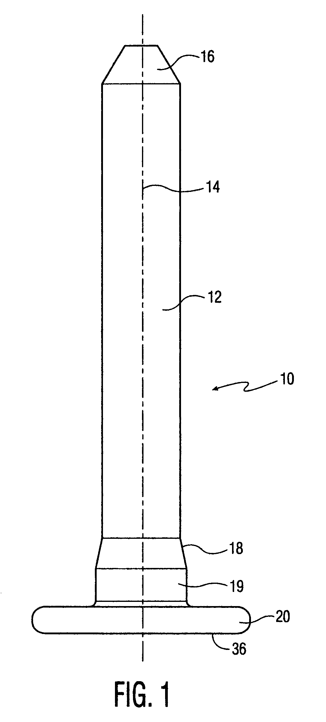
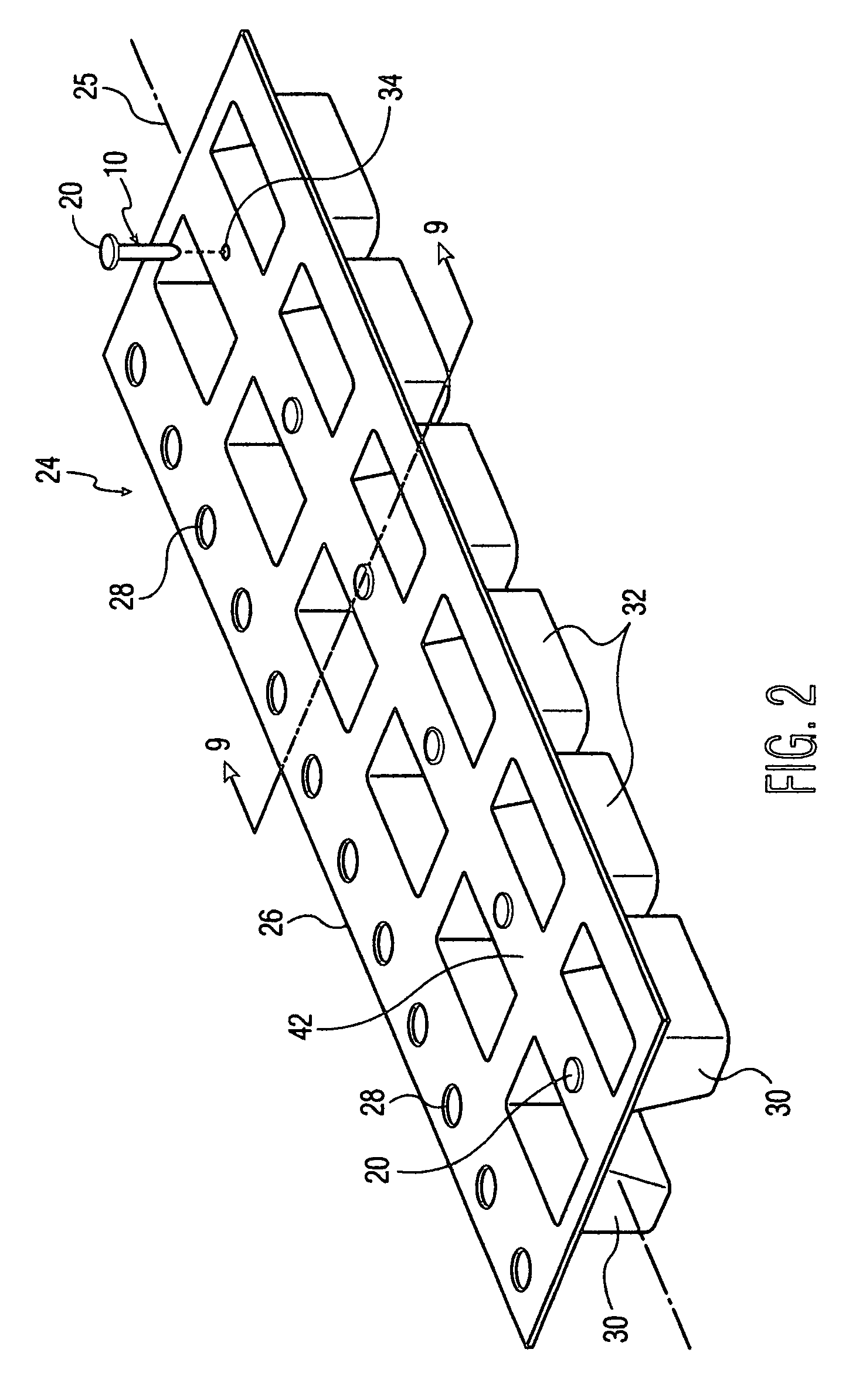
[0026]FIG. 1 illustrates one form of round pin member comprising an elongated shank section having a central axis and topped off with a larger diameter head. Between the head and the shank is an intermediate tapered section whose outer diameter tapers outwardly from that of the shank. The most important application of the invention is the provision of metal pins for mounting by standard SMT placement equipment into holes of a PCB or other substrate. However, the invention is not limited to metal pins, nor to PCBs. The invention can be used with any kind of substrate that has openings into which a projecting member needs to be mounted by placement in the holes. While a common purpose would be to establish an electrically-conductive contact between an electrically-conductive portion on the contact member and an electrically-conductive part o...


PUM


Abstract

A non-intrusive surface mount interconnect that provides a through-hole interconnect to the opposite side of a PCB board. A headed pin (head up / shank down) can be picked by standard placement equipment from a specially configured pocket tape using a hole that is tightly controlled for pin location. The head of the pin rests on top of the packaging tape preventing the pin from passing through the hole. A tapered section on the pin fits with minimal clearence assuring that a vacuum nozzle on the placement equipment when it descends sees and contacts the head top for vacuum nozzle pick-up.

Description

[0001]The invention is directed to a solid through-hole pin for solder attaching into a preformed hole in a substrate, such as a printed circuit board (PCB) or the like.BACKGROUND OF INVENTION[0002]There are several approaches used in the electronic industry today that address how to solder attach a contact such as a pin to a PCB or other substrate (e.g., FR-4, ceramic, plastic, Teflon, metal etc.) using a solder paste and reflow process. These approaches include:[0003]1. Interference Fit Pin Through Paste: This scheme uses a pin with an interference fit, such as when the pin is square and interferes with a round hole or has a protrusion / interference section along the shank of a round or square pin. The square pin or the interference section provides an interference fit when inserted into a hole of a PCB. Pre-deposited solder paste in or around the hole that the pin is inserted into provides a preferred solder joint when reflowed as would a secondary wave solder process. A problem w...

Claims


Application Information

Patent Timeline
Patent Type & Authority Patents(United States)
IPC IPC(8): B65D85/20B65D85/24H01R43/20H05K13/00
CPCH05K13/0084H01R12/58H01R43/205Y10S206/82
Inventor KENNEDY, CRAIG M.TORIGIAN, GREGORY K.
Owner AUTOSPLICE SYST
Why Eureka
Try Eureka