Seal ring structure for radio frequency integrated circuits

a technology of integrated circuits and sealing rings, applied in the direction of semiconductor devices, semiconductor/solid-state device details, electrical devices, etc., can solve the problems of signal distortion, unwanted signal interference at one time, etc., to reduce cross coupling between circuits and pads, prevent cross coupling, and reduce unwanted signal coupling

Inactive Publication Date: 2005-11-22
TAIWAN SEMICON MFG CO LTD
View PDF11 Cites 25 Cited by
  • Summary
  • Abstract
  • Description
  • Claims
  • Application Information

AI Technical Summary

Benefits of technology

[0009]A principal object of the present invention is to provide a method that reduces cross coupling between circuits and pads in an integrated circuit.
[0010]Another object of the present invention is to provide a method that prevents cross coupling between circuits caused by the seal ring in an integrated circuit.
[0011]These objects are achieved by using a method where a seal ring is formed by stacking interconnected metal layers along the perimeter of the integrated circuit (IC). Discontinuities are formed in the seal ring encapsulating different sections of the IC. There are no overlaps between discontinuities in the seal ring thus isolating signals utilized on different sub-circuits within the IC. To further reduce unwanted signal coupling, the distances between the seal ring and both signal pads and circuits are enlarged. Electrical connection is made between the deep N-well and the seal ring to encapsulate the substrate and minimized signal coupling to the substrate.

Problems solved by technology

One problem with this method is that signals from the bonding pads 24 may be capacitively coupled to the seal ring 22.
This may result in unwanted signal interference appearing at one of the signal input or output bonding pads 24.
In addition, interference may be coupled to the RF circuit 26 resulting in signal distortion.

Method used


Image

  • Seal ring structure for radio frequency integrated circuits
  • Seal ring structure for radio frequency integrated circuits
  • Seal ring structure for radio frequency integrated circuits

Examples


Embodiment Construction

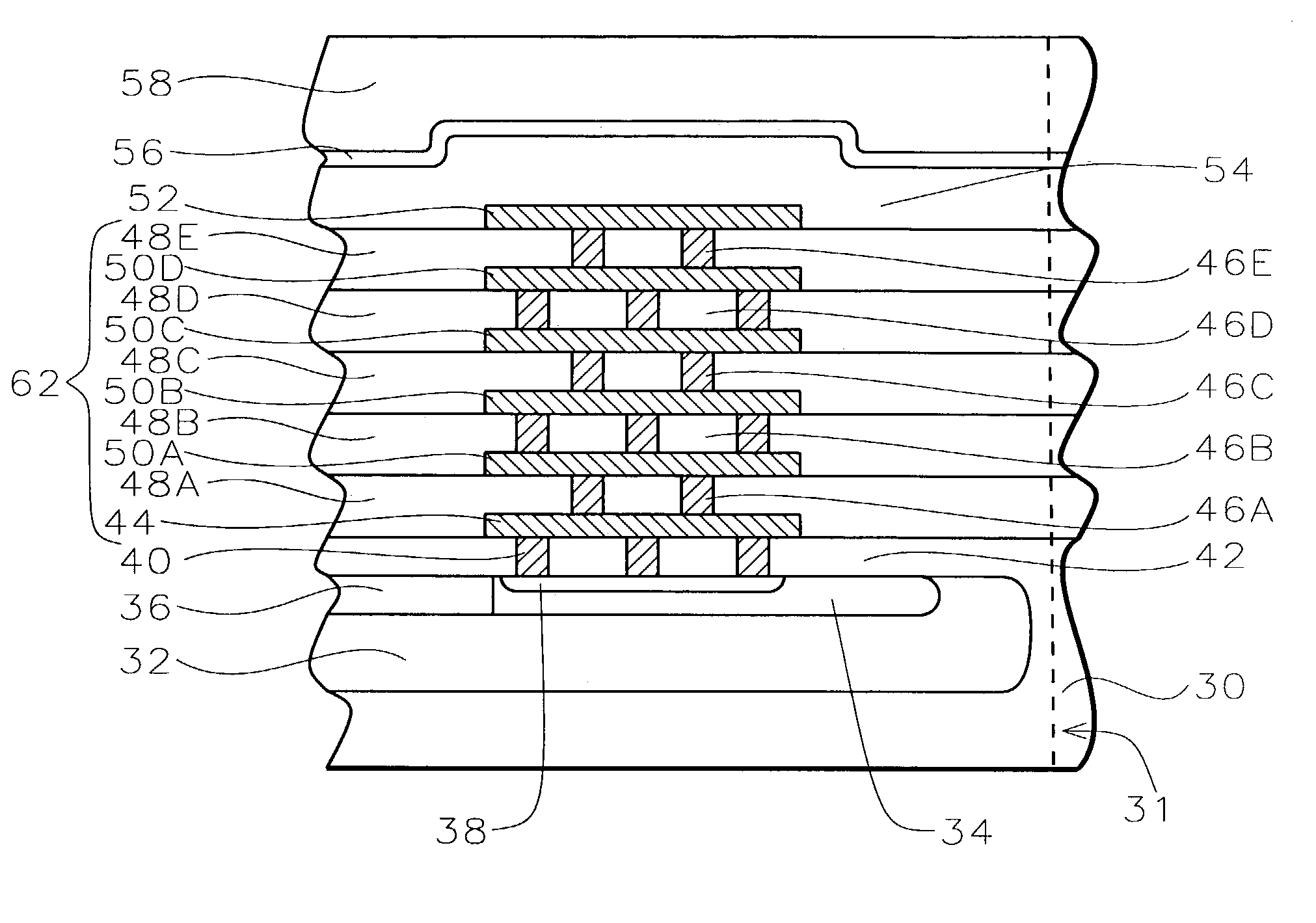
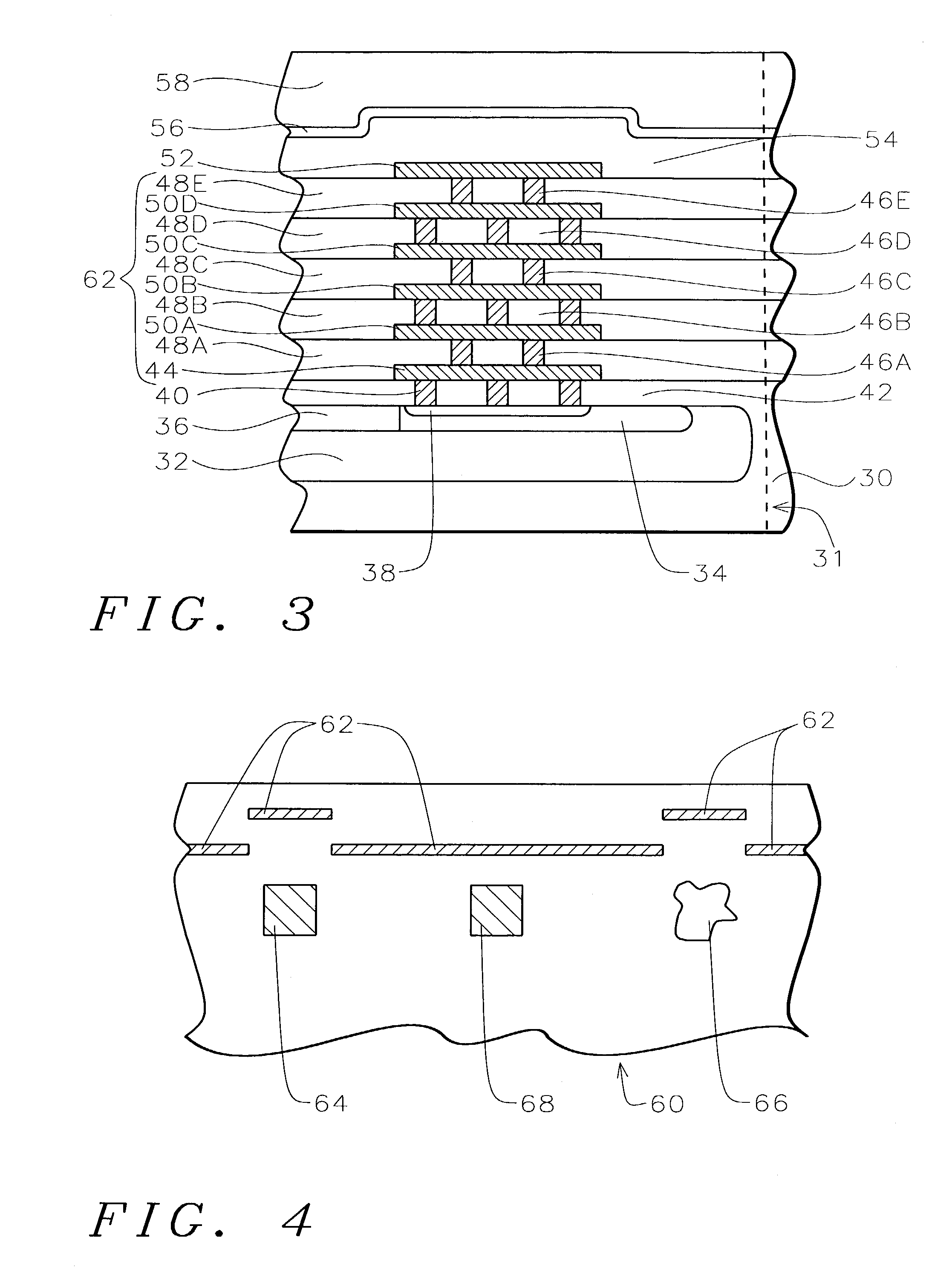
[0017]The present invention uses a method where a seal ring is formed by stacking interconnected conducting layers along the perimeter of the integrated circuit (IC). The embodiment provided herein describes a method of creating the seal ring and connecting the seal ring to the deep N-well.

[0018]Refer to FIG. 3, depicting in cross-section a portion of an integrated circuit die where the seal ring is formed. A substrate 30 is provided. The substrate layer 30 may contain underlying layers, devices, junctions, and other features (not shown) formed during prior process steps. The cut line 31 represents the outer edge of the IC die of interest. During subsequent processing, the die would be separated from an adjacent IC die (not shown) on the substrate 30 along that cut line 31. A deep N-well region 32 is formed as is conventional in the art. A p+source / drain (S / D) region 34 formed by conventional techniques is isolated from the remainder of the underlying circuitry (not shown) by shallo...


PUM


Abstract

Described is a method wherein a seal ring is formed by patterning multiple layers each comprised of a dielectric layer with conductive vias covered by a conductive layer. Discontinuities are made in the seal ring encapsulating an integrated circuit. There are no overlaps between different sections of the seal ring thereby reducing coupling of high frequency circuits in the seal ring structures. In addition, the distance between signal pads, circuits and the seal ring are enlarged. Electrical connection is made between deep N-wells and the seal ring. This encapsulates the integrated circuit substrate and reduces signal coupling with the substrate.

Description

[0001]This is a division of U.S. patent application Ser. No. 09 / 933,965, filing date Aug. 22, 2001 now U.S. Pat. No. 6,537,849, Seal Ring Structure For Radio Frequency Integrated Circuits, assigned to the same assignee as the present invention.BACKGROUND OF THE INVENTION[0002](1) Field of the Invention[0003]The invention generally relates to an encapsulation process used in semiconductor manufacturing and, more particularly, to a method of encapsulation that improves isolation of radio frequency (RF) signals in the fabrication of integrated circuits.[0004](2) Description of Prior Art[0005]As integrated circuit (IC) speeds increase, seal rings have been incorporated into the device encapsulation in order to reduce radio frequency (RF) interference and signal cross coupling. The seal ring is grounded or connected to a signal ground such as a DC supply line to eliminate the effect of interference. The seal ring may be part of the device packaging scheme; in this case a conductive lid i...

Claims


Application Information

Patent Timeline
Patent Type & Authority Patents(United States)
IPC IPC(8): H01L21/48H01L21/50H01L23/02H01L21/00H01L21/02H01L21/44H01L23/552H01L23/58
CPCH01L23/552H01L23/585H01L2924/01322H01L24/05H01L2924/00014H01L2224/05599H01L2924/14H01L2924/00
Inventor TSAI, CHAO-CHIEHWONG, SHIH CHIH
Owner TAIWAN SEMICON MFG CO LTD
Why Eureka
Try Eureka