
Semiconductor device and portable electronic apparatus

a technology of semiconductor devices and electronic equipment, applied in the direction of semiconductor devices, semiconductor/solid-state device details, electrical equipment, etc., can solve the problems of increased power consumption, low circuit operating speed, and increased off-leak current of mosfets, so as to prolong the battery life to a large extent, the effect of less power consumption

Inactive Publication Date: 2005-11-29
SHARP KK
View PDF13 Cites 7 Cited by
  • Summary
  • Abstract
  • Description
  • Claims
  • Application Information

AI Technical Summary

Benefits of technology

[0021]The present invention having been accomplished with a view to solving these problems, it is therefore an object of the invention to provide a low-power-consumption, high-reliability semiconductor device having DTMOS' and substrate-bias variable transistors, as well as portable electronic equipment using the semiconductor device.

Problems solved by technology

However, merely lowering the power supply voltage would cause the drive current of MOSFETs to lower, resulting in a lower operating speed of the circuit.
Although this phenomenon can be prevented by lowering the threshold, doing so would give rise to a problem of increases in off-leak current of MOSFETs.
As a result, the power consumption would increase.
That is, a very large electrostatic capacity is parasitically present.
. . causes the bias of the whole N-type deep well region 312 to change, which in turn causes large amounts of charges to be charged and discharged.
As a result, the power consumption increases.
Thus, largely changing bias of the N-type deep well region 312 makes it difficult to control the latch-up phenomenon.
As a result, the device reliability deteriorates.

Method used


Image

  • Semiconductor device and portable electronic apparatus
  • Semiconductor device and portable electronic apparatus
  • Semiconductor device and portable electronic apparatus

Examples


Embodiment Construction

[0104]Hereinbelow, the present invention is described in detail by way of embodiments thereof illustrated in the accompanying drawings.

[0105]Semiconductor substrates usable for the present invention, although not particularly limited, are preferably silicon substrates. The semiconductor substrate may have either conductive type, P-type or N-type.

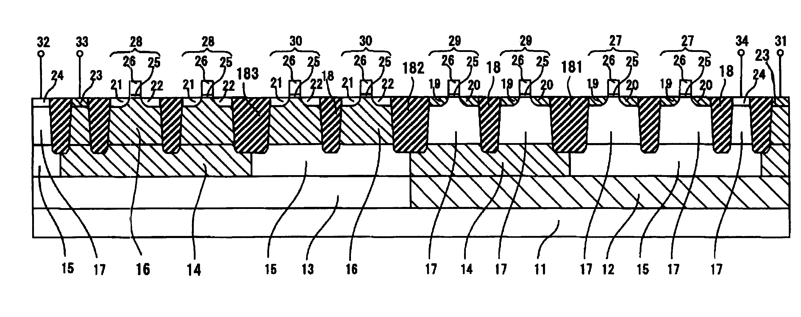
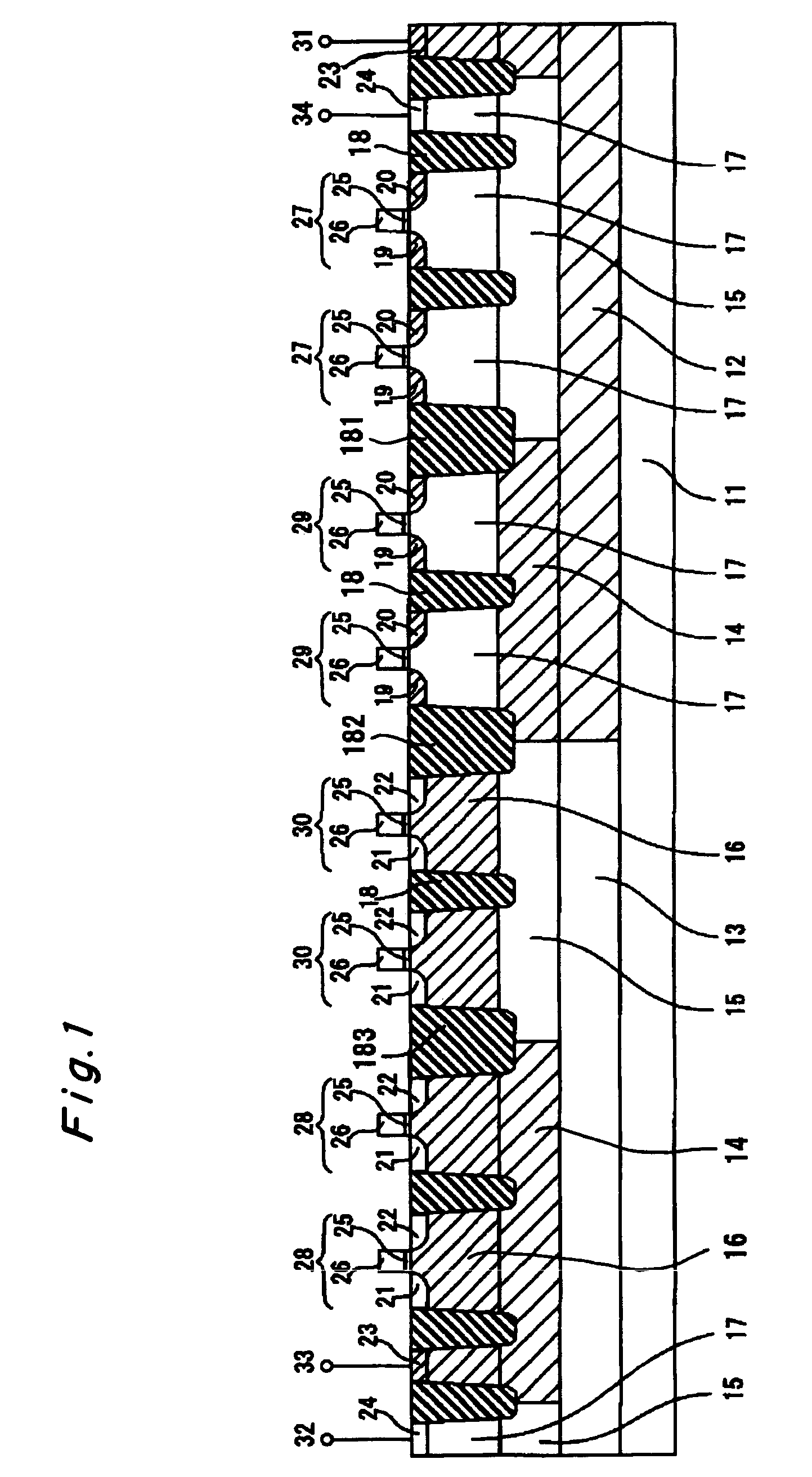
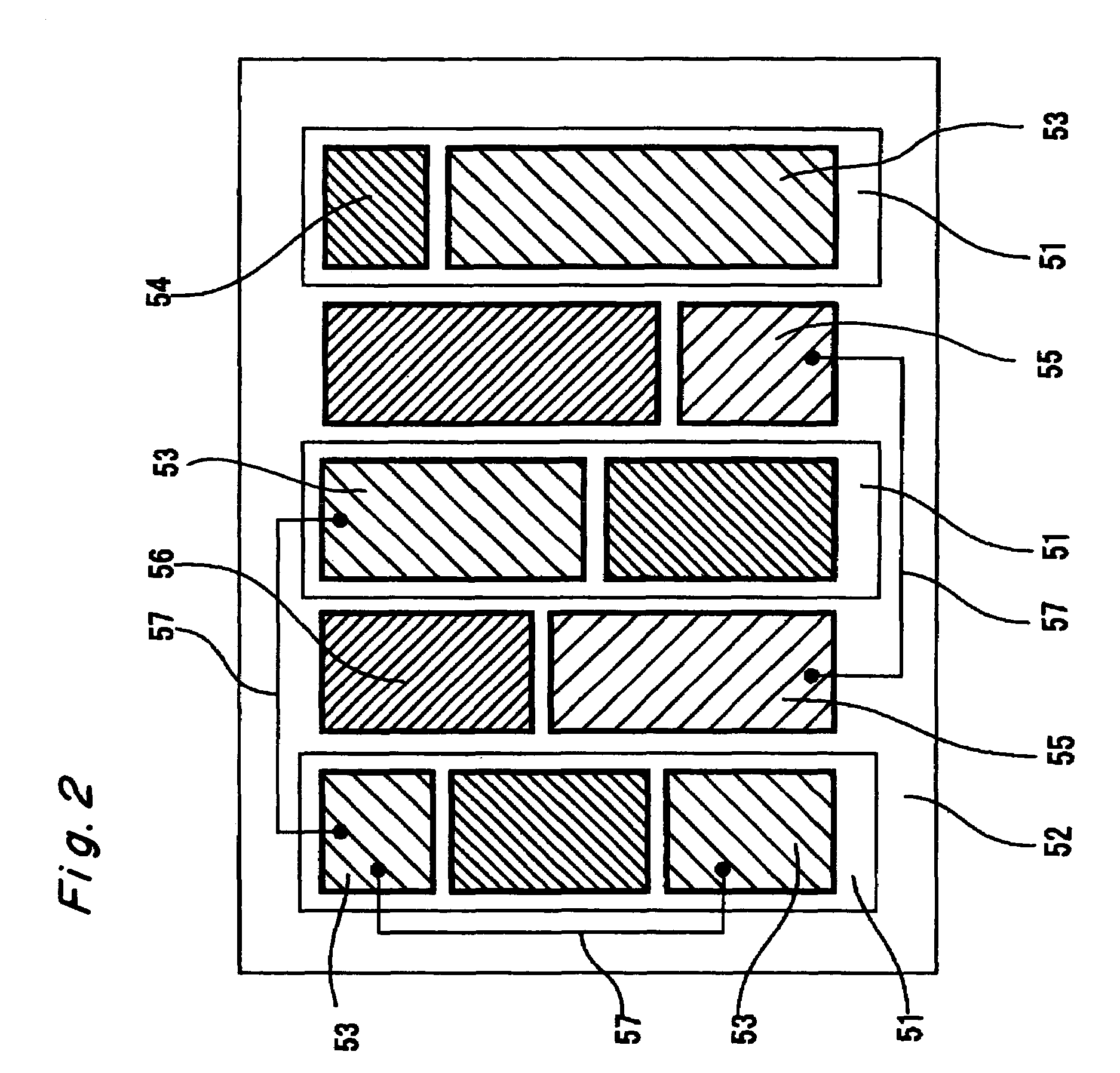
[0106]FIG. 1 is a cross-sectional schematic view of a semiconductor device according to an embodiment of the invention, and FIG. 2 is a plan schematic view of the semiconductor device.

[0107]As shown in FIG. 1, in this semiconductor device, an N-type very deep, i.e. first deepest, well region 12 and a P-type very deep, i.e. first deepest, well region 13 are formed in a P-type silicon substrate 11.

[0108]An N-type deep, i.e. second deepest, well region 14 is formed in the N-type very deep well region 12. A P-type shallow well region 17 is formed in the N-type deep well region 14. An N-type source region 19 and an N-type drain region 20 are form...


PUM


Abstract

There is provided a semiconductor device of low power consumption and high reliability having DTMOS' and substrate-bias variable transistors, and portable electronic equipment using the semiconductor device. On a semiconductor substrate (11), trilayer well regions (12, 14, 16; 13, 15, 16) are formed, and DTMOS' (29, 30) and substrate-bias variable transistors (27, 28) are provided in the shallow well regions (16, 17). Large-width device isolation regions (181, 182, 183) are provided at boundaries forming PNP, NPN or NPNP structures, where a small-width device isolation region (18) is provided on condition that well regions on both sides are of an identical conductive type. Thus, a plurality of well regions of individual conductive types where substrate-bias variable transistors (27, 28) of individual conductive types are provided can be made electrically independent of one another, allowing the power consumption to be reduced. Besides, the latch-up phenomenon can be suppressed.

Description

[0001]This application is the national phase under 35 U.S.C. § 371 of PCT International Application No. PCT / JP01 / 09887 which has an International filing date of Nov. 13, 2001, which designated the United States of America.TECHNICAL FIELD[0002]The present invention relates to semiconductor devices and portable electronic equipment, and more specifically to a semiconductor device having a dynamic threshold transistor and a substrate-bias variable transistor, as well as portable electronic equipment using this semiconductor device.BACKGROUND ART[0003]In order to decrease power consumption in CMOS (Complementary Metal Oxide Semiconductor) circuits using MOSFETs (Metal Oxide Semiconductor Field Effect Transistors), it is most effective to lower the power supply voltage. However, merely lowering the power supply voltage would cause the drive current of MOSFETs to lower, resulting in a lower operating speed of the circuit. This phenomenon is known to become noticeable as the power supply v...

Claims


Application Information

Patent Timeline
Patent Type & Authority Patents(United States)
IPC IPC(8): H01L21/762H01L21/76H01L21/8234H01L21/8238H01L27/08H01L27/088H01L27/092
CPCH01L21/76229H01L21/823892H01L27/092H01L27/0921H01L29/78
Inventor SHIBATA, AKIHIDEIWATA, HIROSHIKAKIMOTO, SEIZO
Owner SHARP KK
Learn More