

Methods of redundancy in a floating trap memory element based field programmable gate array
a technology of programmable gate array and memory element, which is applied in the field of providing redundancy for floating trap configuration memory elements, can solve the problems of electrons tunneling off of floating gates, additional columns or rows are provided at the expense of reducing the available logic resources in the pld
- Summary
- Abstract
- Description
- Claims
- Application Information
AI Technical Summary
Problems solved by technology
Method used
Image

Examples
first embodiment
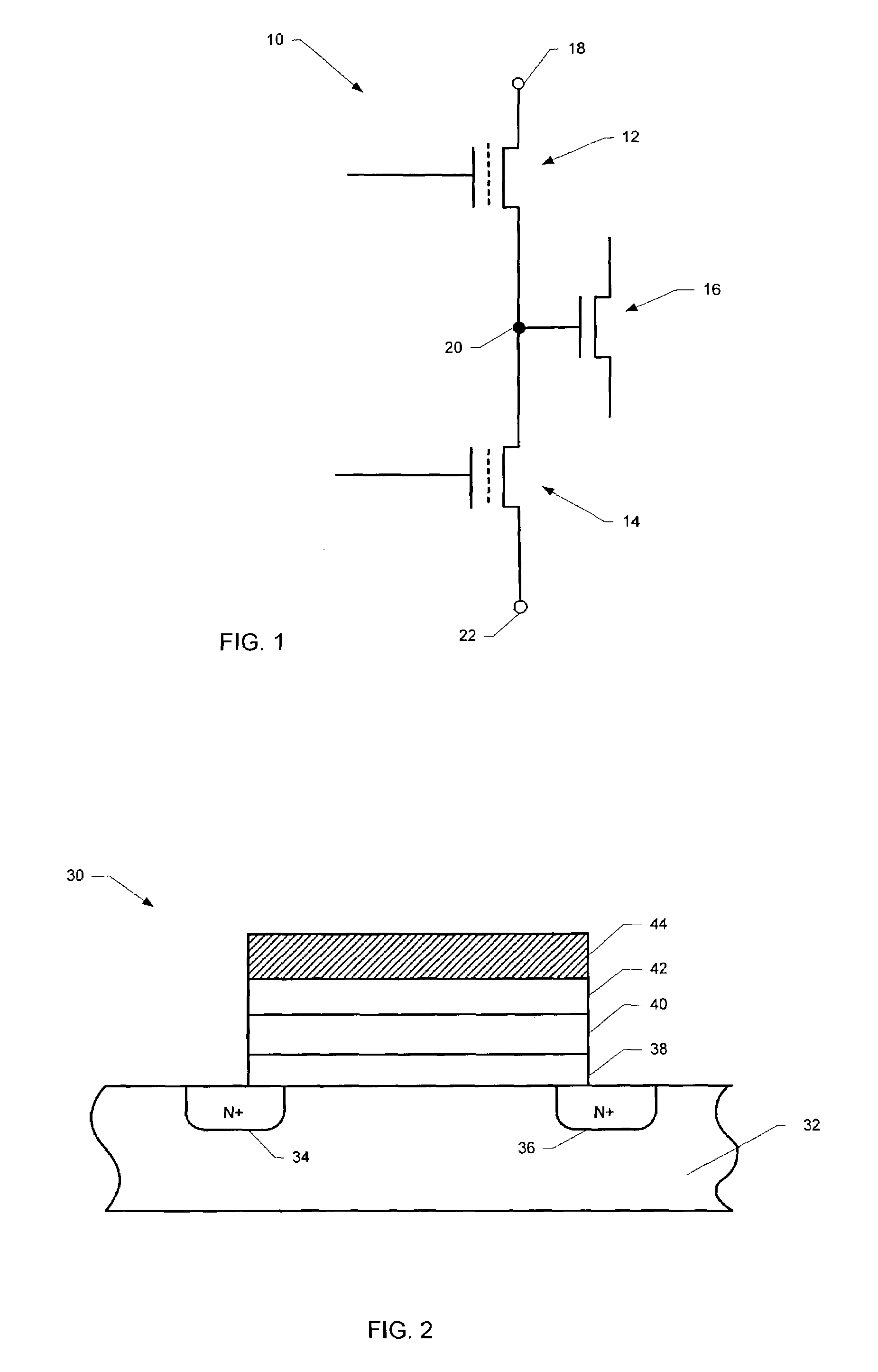
[0039]FIG. 4 is a flow diagram illustrating the steps of a redundancy scheme according to the present invention. In step 50 the charge in the trapping layer in a first area above either the source or the drain of n-channel MOS charge trapping transistor 12 is read (sensed) along with the charge above the opposite junction of n-channel MOS charge trapping transistor 14. For example, if the charge above the drain junction of n-channel MOS charge trapping transistor 12 is read, then the charge above the source junction of n-channel MOS charge trapping transistor 14 will also be read. Otherwise, if the charge above the source junction of n-channel MOS charge trapping transistor 12 is read, then the charge above the drain junction of n-channel MOS charge trapping transistor 14 will also be read.
[0040]Preferably, in this manner, the charge on both n-channel MOS charge trapping transistors 12 and 14 may be read simultaneously. In FIG. 5, the areas above the opposite junctions which may be ...
second embodiment
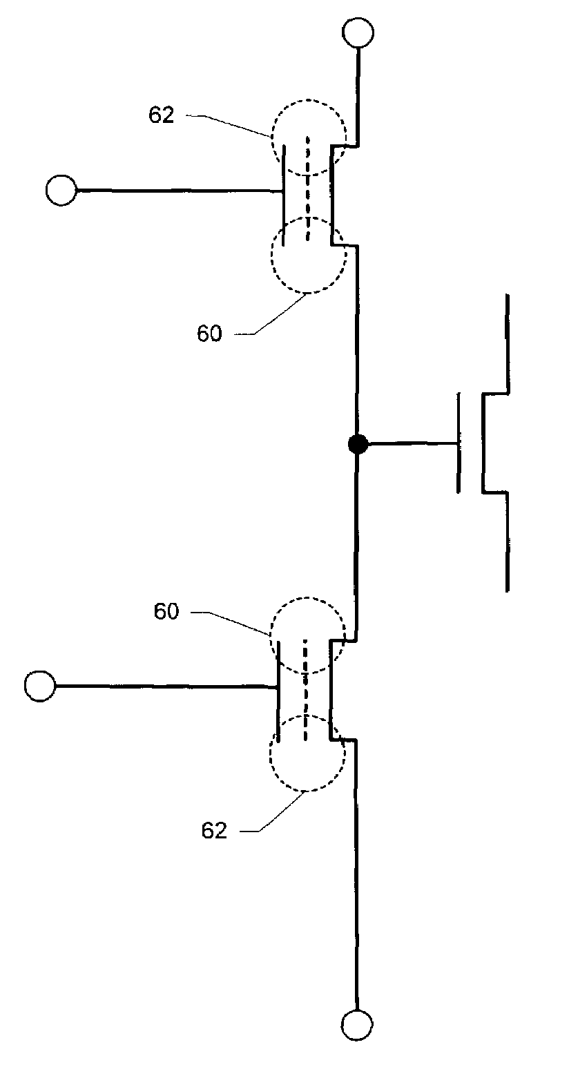
[0044]FIG. 6 is a flow diagram illustrating the steps of a redundancy scheme according to the present invention. In step 60, the charge above the junctions of the n-channel MOS charge trapping transistors 12 and 14 is read. In step 62, it is determined whether the n-channel MOS charge trapping transistors 12 or 14 have been adequately programmed by channel hot electron injection. In step 64, when the programming of either of the n-channel MOS charge trapping transistors 12 or 14 is inadequate in step 62, the charge trapping layer of the inadequately programmed n-channel MOS charge trapping transistor 12 or 14 is programmed by Fowler-Nordheim tunneling.
[0045]As described above, for channel hot electron injection programming of the area above the source / drain junctions of an n-channel MOS charge trapping transistor, the gate of the MOS transistor in the n-channel MOS charge trapping transistor is held at a first potential, typically about 8 to about 12 volts greater than a second pote...
third embodiment
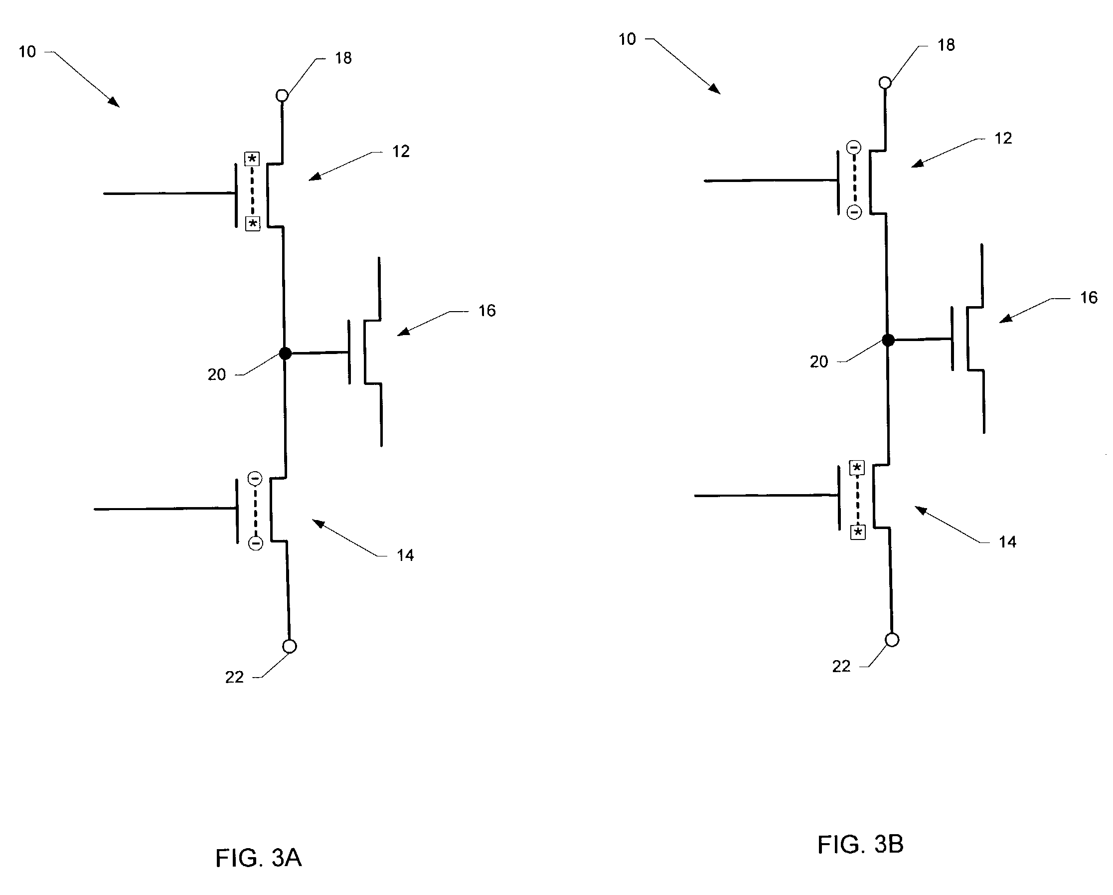
[0048]FIG. 7 is a flow diagram illustrating the steps of a redundancy scheme according to the present invention. In step 70, the charge above the junctions of the n-channel MOS charge trapping transistors 12 and 14 is read. In step 72, it is determined whether the n-channel MOS charge trapping transistors 12 or 14 have been adequately erased by tunneling enhanced channel hot hole injection. In step 74, when the erasure of either of the n-channel MOS charge trapping transistors 12 or 14 is inadequate in step 72, the charge trapping layer of the inadequately erased n-channel MOS charge trapping transistor 12 or 14 is erased by Fowler-Nordheim tunneling.
[0049]As described above, for tunneling enhanced hot hole injection erasure of one of the areas above the source / drain junctions of an n-channel MOS charge trapping transistor, the gate of the MOS transistor in the n-channel MOS charge trapping transistor is held at a first potential, typically about 8 to about 12 volts less than a seco...
PUM
 Abstract
Description
Claims
Application Information