System and method for assured built in self repair of memories

a self-repair and memory technology, applied in the field of computer memory, can solve the problems of increasing the risk of such defects in embedded memories, the quantity of memory, and the defects of various types, and achieve the effects of reducing the pulse width, facilitating the discovery of weak memory cells as well as faulty memory cells

Inactive Publication Date: 2005-12-06
ARM INC
View PDF14 Cites 32 Cited by
  • Summary
  • Abstract
  • Description
  • Claims
  • Application Information

AI Technical Summary

Benefits of technology

The present invention provides a system and method for detecting and repairing defective memory cells in a computer chip. The system uses a stress clock signal with a decreased pulse width to detect both faulty and weak memory cells. The stress clock signal is used during power up of the chip and is followed by a built-in self-test that stores defective memory addresses in a register. The chip's internal clock signal is used during normal memory access operations, while the stress clock signal is used for the built-in self-test. The system can also include redundant control logic that redirects memory access operations to redundant memory cells for the repair of defective memory addresses. The invention allows for the detection and repair of weak memory cells, improving the reliability of computer chips.

Problems solved by technology

The technical problem addressed in this patent text is the need for improved built-in self-repair methods to repair defective memory cells in IC or SOC chips. The current methods of repairing using laser fuses or other hard-walled methods are limited in their effectiveness and may not identify all the weak cells. This method aims to provide a more effective solution for repairing embedded memories in IC or SOC chips.

Method used


Image

  • System and method for assured built in self repair of memories
  • System and method for assured built in self repair of memories
  • System and method for assured built in self repair of memories

Examples


Embodiment Construction

[0035]An invention is disclosed for ensuring built-in self-repair to a memory. To this end, the embodiments of the present invention provide built-in self-repair systems that test the memory array at a high stress level to discover weak memory cells, as well as faulty memory cells. In the following description, numerous specific details are set forth in order to provide a thorough understanding of the present invention. It will be apparent, however, to one skilled in the art that the present invention may be practiced without some or all of these specific details. In other instances, well known process steps have not been described in detail in order not to unnecessarily obscure the present invention.

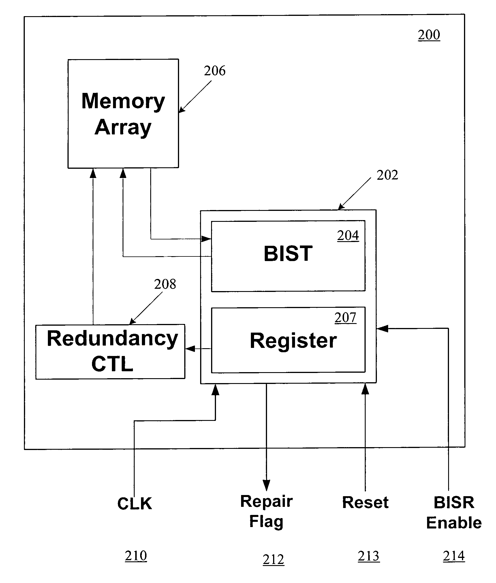
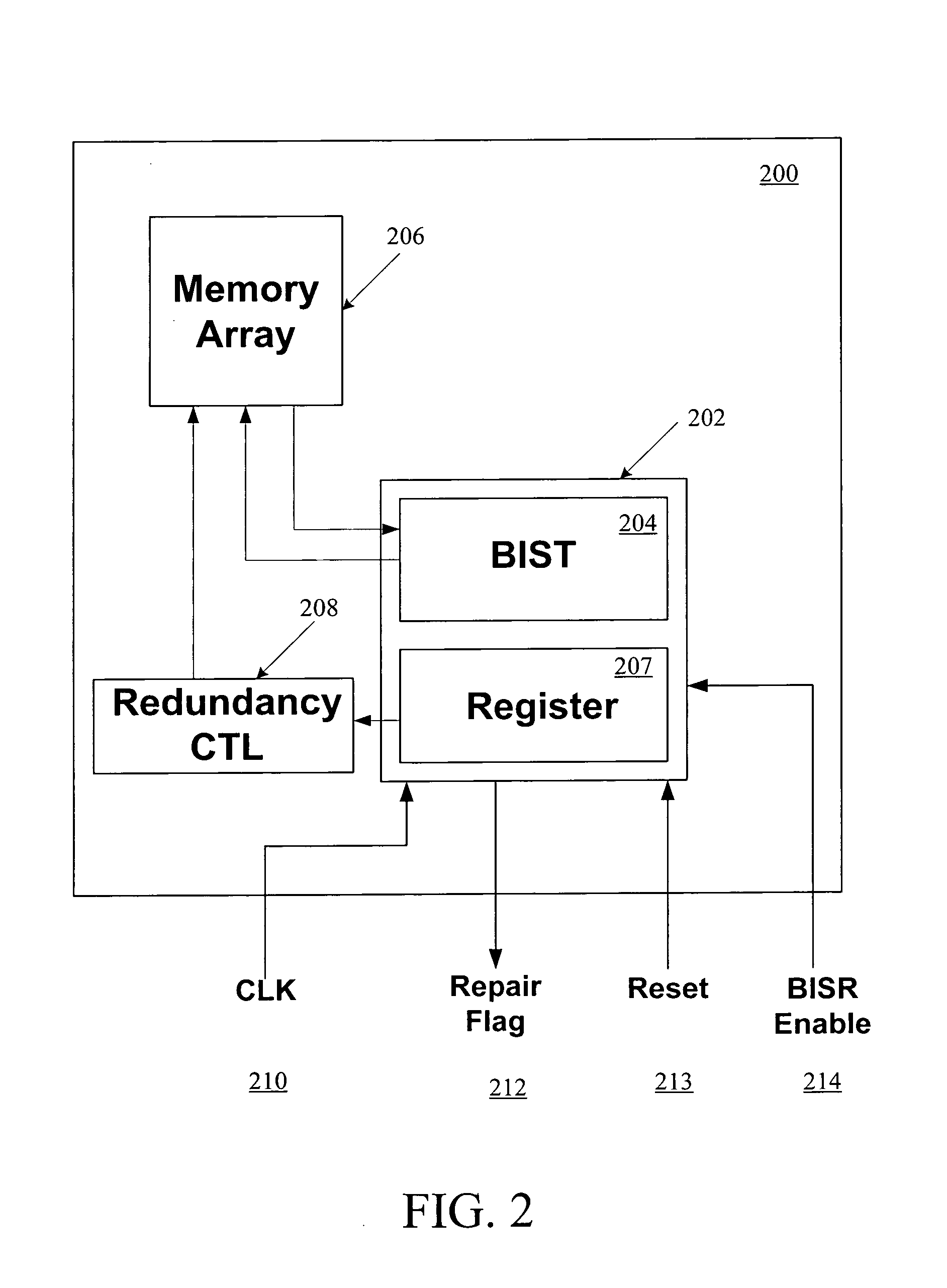
[0036]FIG. 1 has been described in terms of the prior art. FIG. 2 is a block diagram of embedded memory system 200 with high stress built-in self-repair, in accordance with an embodiment of the present invention. The memory system 200 can be implemented entirely on one IC or SOC, or on ...


PUM


Abstract

An embedded memory device having improved BISR capabilities is provided. The embedded memory device includes an internal clock signal for use in accessing a memory array having access to redundant memory cells during normal operation, and a stress clock signal, wherein each pulse of the stress clock signal is of a shorter duration than each pulse of the internal clock signal. Further included are a built-in self-test circuit that performs a built-in self-test using the stress clock signal, and a register that stores defective memory addresses detected by the built-in self-test circuit. Redundant control logic is also included that redirects memory access operations to the defective memory addresses to redundant memory cells.

Description


Claims


Application Information

Patent Timeline
Owner ARM INC
Why Eureka
Try Eureka