Reactor precoating for reduced stress and uniform CVD

a precoating and reactor technology, applied in the field of semiconductor processing, can solve the problems of unacceptably high particle levels in the process tube, large disadvantages of the btbas process, and only economical manufacturing processes, and achieve the effect of increasing and maintaining the deposition ra

Inactive Publication Date: 2005-12-13
ASM INTERNATIONAL
View PDF56 Cites 411 Cited by
  • Summary
  • Abstract
  • Description
  • Claims
  • Application Information

AI Technical Summary

Benefits of technology

[0004]In accordance with one aspect of the invention, a method is provided to reduce the loss in deposition rate following the cleaning of a reaction chamber comprising the steps of: cleaning the reaction chamber; precoating the reaction chamber with silicon nitride using an inorganic silicon reactant and a nitrogen source; and depositing silicon nitride on a workpiece using an organic silicon reactant.
[0007]An advantage of the preferred embodiments is to provide a method for the operation of a reaction chamber for the deposition of nitride films using BTBAS and ammonia as precursors, that allows for the performance of an economically feasible number of production runs between cleaning cycles. Another advantage is that the pre-coating method is effective for increasing and maintaining the deposition rate of low temperature depositions, following a cleaning of the reaction chamber.

Problems solved by technology

However, this BTBAS process has a large disadvantage.
After a few deposition runs, or a limited cumulative film thickness of about 300 nm on the quartz process tube and the quartz wafer boat, the particle levels in the process tube start to increase to unacceptably high levels.
Due to the high frequency of cleaning, this manufacturing process is only economical when the cleaning can be performed in-situ, by feeding a cleaning gas into the process tube, without a need to dismount the process tube for each cleaning.
Unfortunately, after cleaning with NF3, the deposition rate of the BTBAS process appears to be significantly lower than before the cleaning, perhaps due to undesirable roughening of the exposed quartz surfaces.
Thus, using BTBAS is counter-productive since it reduces the number of production runs that can be performed between cleanings.

Method used


Image

  • Reactor precoating for reduced stress and uniform CVD
  • Reactor precoating for reduced stress and uniform CVD

Examples


Embodiment Construction

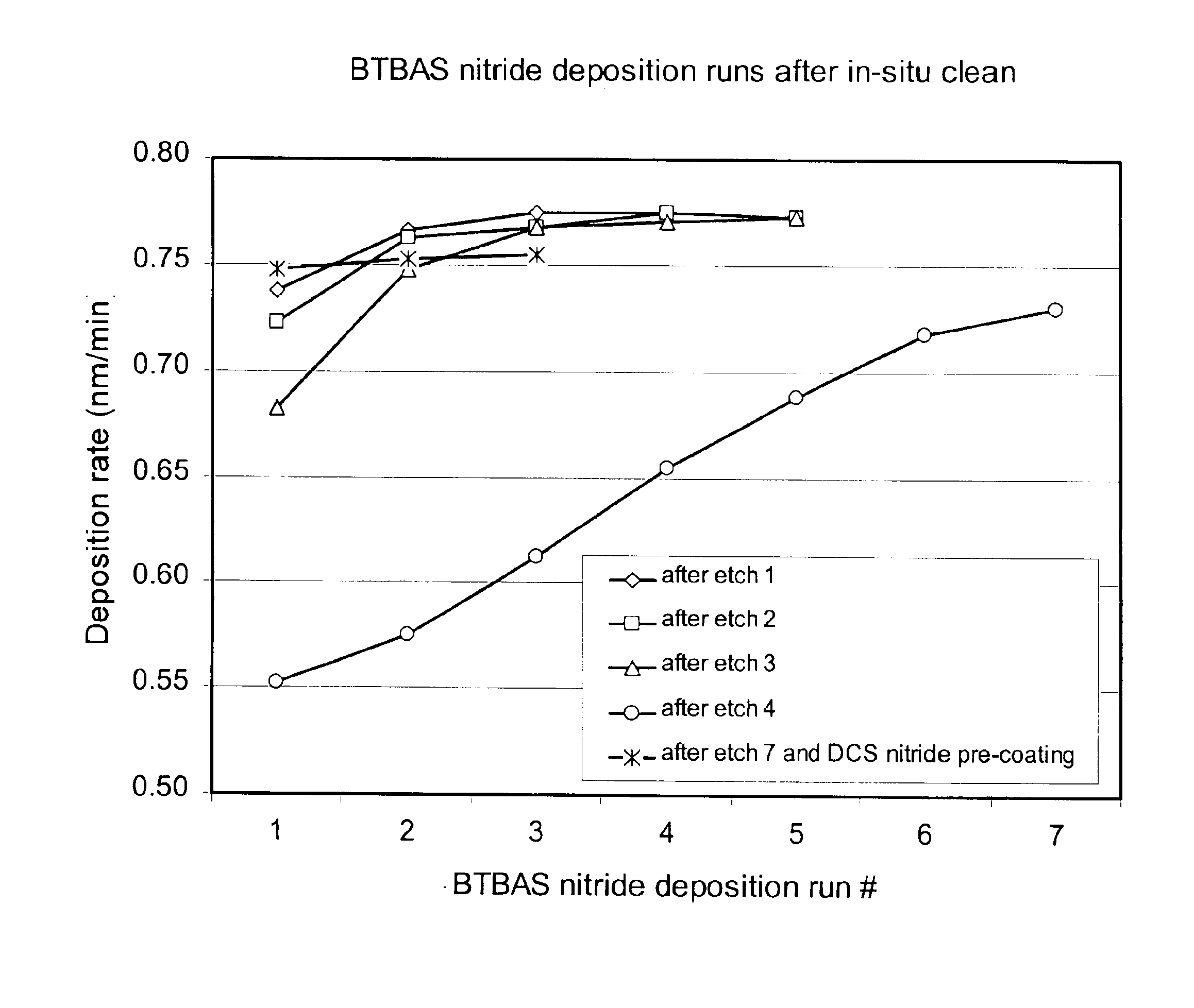
[0009]In one embodiment, a method is provided for deposition of silicon nitride films workpieces or substrates in a plurality of runs using an organic silicon source, and particularly bis-tertiary-butyl amino silane (BTBAS). This embodiment will be described in further detail with reference to FIG. 1. FIG. 1 shows the deposition rate for a series of consecutive BTBAS-based nitride deposition runs. Prior to each series, an in-situ cleaning was performed on the quartz process tube and the quartz wafer boat that accommodates the wafers in a vertically spaced relationship. Quartz rings were disposed directly below each wafer to improve the uniformity of the BTBAS-based deposition over each wafer. At the start of the experiments shown in FIG. 1, the quartzware was new and unused. A first series of four depositions of a thickness of 60 nm to 80 nm each was carried out. During this series the process conditions, in particular the temperatures of five heating zones in a vertical batch proce...


PUM

PropertyMeasurementUnit
temperatureaaaaaaaaaa
thicknessaaaaaaaaaa

Abstract

A method is provided for obtaining stable and elevated deposition rates in a reaction chamber, following the cleaning of the chamber. The method involves cleaning of the chamber, pre-coating the interior surfaces of the reaction chamber with an inorganic composition, and then, using the pre-coated chamber to deposit an organic layer onto a workpiece.

Description

FIELD OF THE INVENTION[0001]The invention relates generally to the field of semiconductor processing; and more particularly, to the field of nitride film deposition on semiconductor substrates.BACKGROUND OF THE INVENTION[0002]Recently, a process for the low pressure chemical vapor deposition (LPCVD) of silicon nitride films from ammonia and bis-tertiary-butyl amino silane (BTBAS), having the formula (t-C4H9NH)2SiH2, has been proposed in U.S. Pat. No. 5,874,368 to Laxman. In addition to improved film properties, a significantly lower deposition temperature can be used as compared to a conventional process using ammonia and dichlorosilane (DCS), subjecting the semiconductor substrates to a significantly lower thermal budget. The process is operated in a conventional vertical furnace wherein a plurality of wafers, accommodated in a wafer boat in a horizontal position and in a vertically spaced relationship, are processed in a quartz process tube.[0003]However, this BTBAS process has a ...

Claims


Application Information

Patent Timeline
Patent Type & Authority Patents(United States)
IPC IPC(8): C23C16/34C23C16/44H01L21/314H01L21/318
CPCC23C16/345C23C16/4404C23C16/4405H01L21/3185H01L21/02211H01L21/0217
Inventor TIMMERMANS, ERIC A. H.TEEPEN, MAARTEN J.MUCCIATO, RAFFAELEWILHELM, RUDI
Owner ASM INTERNATIONAL
Why Eureka
Try Eureka