Imaging lens

Active Publication Date: 2005-12-20
TIANJIN OFILM OPTO ELECTRONICS CO LTD
View PDF5 Cites 39 Cited by
  • Summary
  • Abstract
  • Description
  • Claims
  • Application Information

AI Technical Summary

Benefits of technology

[0007]The present invention relates to an imaging lens with optical performance characteristics su

Problems solved by technology

Imaging lenses with only one or two lens elements do not provide adequate optical properties, including correction of aberrations, in the images produced by these devices.
Accordingl

Method used


Image

  • Imaging lens
  • Imaging lens
  • Imaging lens

Examples


Example

Embodiment 1

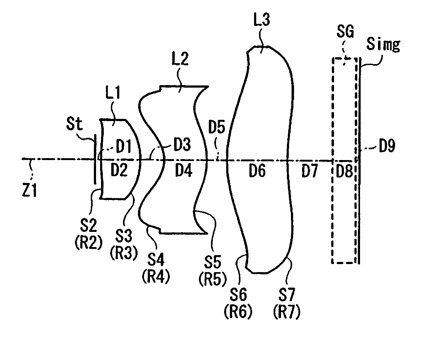
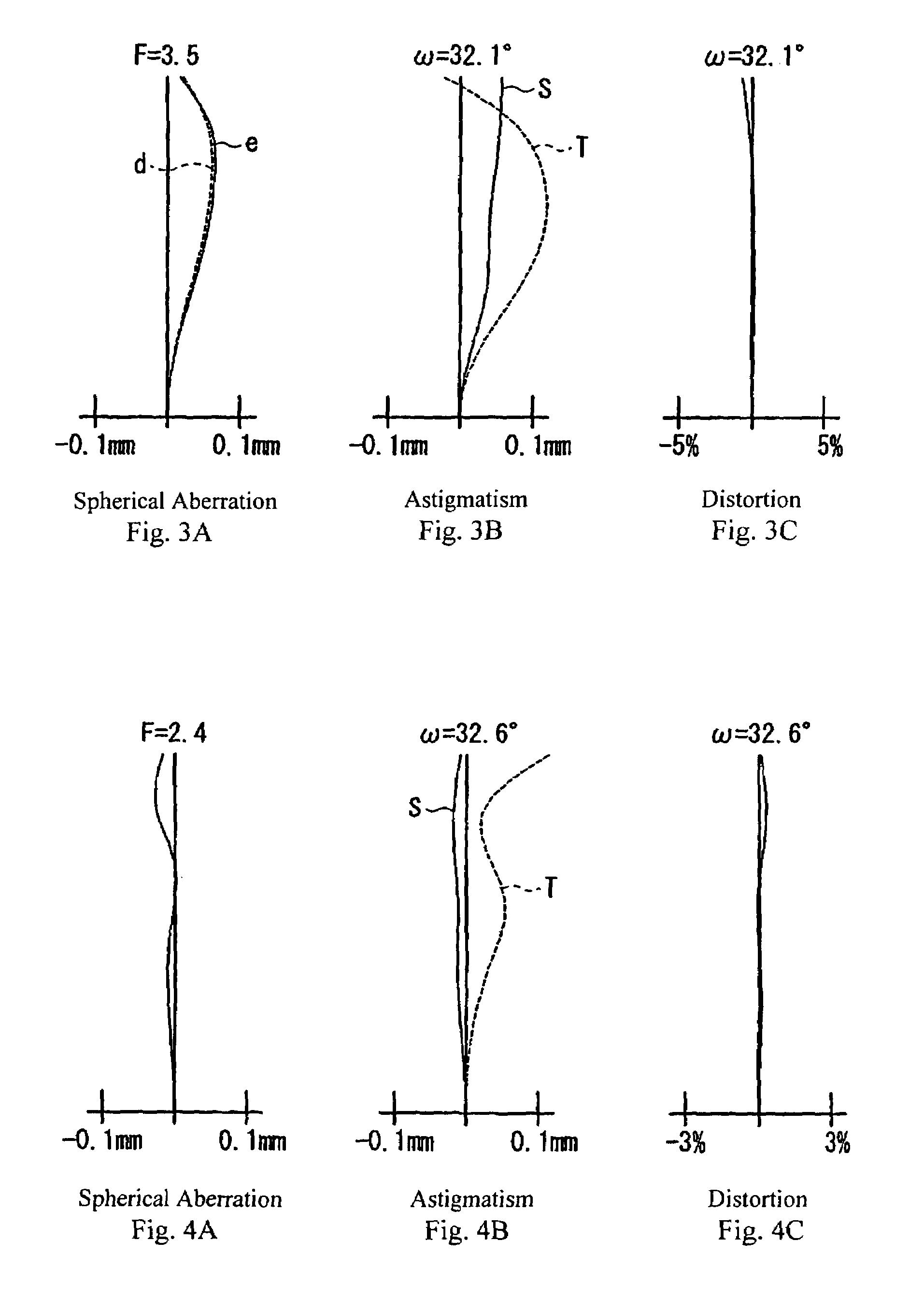
[0041]FIG. 1 shows Embodiment 1 of the present invention. Table 1 below lists the surface number #, in order from the object side, the radius of curvature R (in mm) of each surface near the optical axis, the on-axis surface spacing D (in mm), as well as the refractive index Nd and the Abbe number νd (both at the d-line of 587.6 nm) of each lens element for Embodiment 1. Listed in the bottom portion of Table 1 are the focal length f, the f-number FNO, the maximum image angle 2ω, and the on-axis distance TCL from the diaphragm stop St to the image plane Simg for Embodiment 1. The radius of curvature is infinity (∞) at the planar surfaces of the cover plate SG.

[0042]TABLE 1#RDNdνd1 (stop)∞0.143624.06450.95701.531155.53−1.69280.58354−0.73801.01931.583630.25−1.55620.473462.76431.46871.531155.574.50841.11618∞0.55801.51689∞0.0958f = 4.0 mmFNO = 3.52ω = 64.2°TCL = 6.4 mm

[0043]Table 2 below lists the values of the constants K, and A3–A10 used in Equation (A) above for each of the...

Example

Embodiment 2

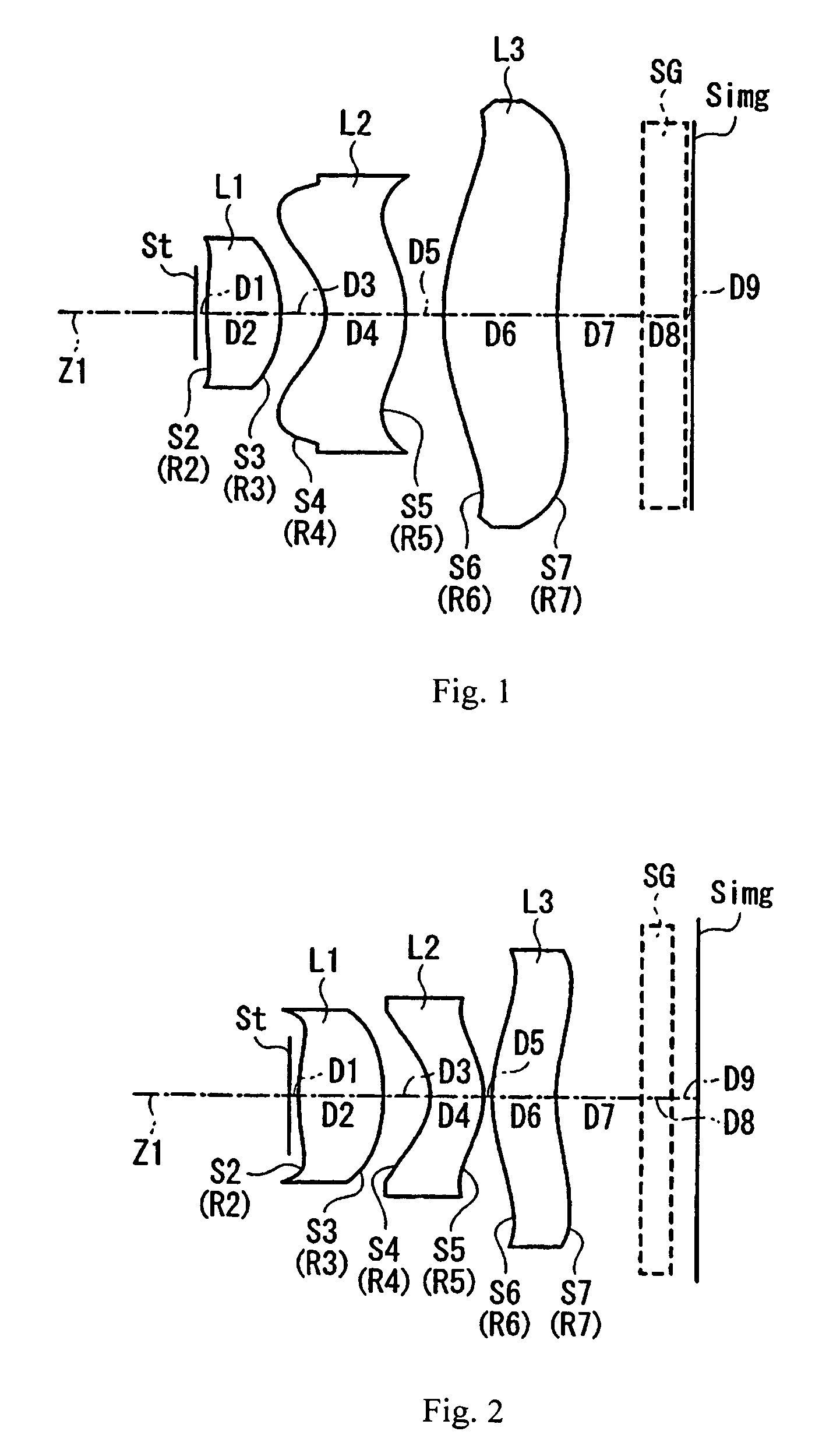
[0049]FIG. 2 shows Embodiment 2 of the present invention. Table 4 below lists the surface number #, in order from the object side, the radius of curvature R (in mm) of each surface near the optical axis, the on-axis surface spacing D (in mm), as well as the refractive index Nd and the Abbe number νd (both at the d-line of 587.6 nm) of each lens element for Embodiment 2. Listed in the bottom portion of Table 4 are the focal length f, the f-number FNO, the maximum image angle 2ω, and the on-axis distance from the diaphragm stop St to the image plane Simg (TCL) for Embodiment 2. The radius of curvature is infinity (∞) at the planar surfaces of the cover plate SG.

[0050]TABLE 4#RDNdνd1 (stop)∞0.126122.86431.11611.531155.53−2.37390.61844−0.65990.68221.583630.25−1.13650.113661.72870.85981.531155.571.91511.15298∞0.40001.51689∞0.3393f = 3.7 mmFNO = 2.42ω = 65.2°TCL = 5.4 mm

[0051]Table 5 below lists the values of the constants K, and A3–A10 used in Equation (A) above for each of t...


PUM


Abstract

An imaging lens for an image pickup device is formed of only three lens components of positive, negative, and positive refractive power, in order from the object side. A diaphragm stop is positioned on the object side of the lens component nearest the object side. Six lens component lens surfaces are aspheric. The lens component nearest the object side is biconvex with regard to the central areas of its two lens surfaces. The image-side surface of the lens component nearest the image side has a concave central area surrounded by a convex surface area. The middle lens component has one lens surface with a concave central area and one lens surface with a convex central area. The Abbe number of the central lens element and the ratio of the focal length of the imaging lens divided by the focal length of the object-side lens component satisfy specified conditions.

Description

BACKGROUND OF THE INVENTION[0001]Imaging devices using image pickup devices such as CCD's (Charge Coupled Devices) and CMOS's (Complementary Metal Oxide Semiconductors) are well known. In such imaging equipment, an image is formed on the image pickup device and electrical signals from the image detector are processed in order to form a viewable image. Recently, along with advancements in miniaturizing the imaging equipment, the entire imaging system has become much smaller.[0002]Video cameras and digital still cameras (hereinafter referred to simply as digital cameras) for image input to cell phones have recently been significantly reduced in size. Imaging lenses used for the small imaging systems used in these devices are conventionally made of a single lens element in view of the small size and portability required.[0003]While imaging devices have been developed to be smaller in recent years, they also have been developed with increasing numbers of pixels in the images. Consequent...

Claims


Application Information

Patent Timeline
IPC IPC(8): G02B9/16G02B13/00G02B13/18G02B13/22
CPCG02B9/16G02B13/0035G02B13/18
Inventor SHINOHARA, YOSHIKAZU
Owner TIANJIN OFILM OPTO ELECTRONICS CO LTD
Why Eureka
Try Eureka