Semiconductor package and method of mounting the same

Inactive Publication Date: 2007-12-20
SAMSUNG ELECTRONICS CO LTD
View PDF13 Cites 5 Cited by
  • Summary
  • Abstract
  • Description
  • Claims
  • Application Information

AI Technical Summary

Benefits of technology

[0007]Some embodiments of the present invention provide a semiconductor package having a good joint between a sealed semiconductor chip and an external board, providing easy measurement of t

Problems solved by technology

However, these methods have many problems.
The solder joint method may use relatively wide areas for interconnections, but when the sealed chip is attached to the external board, solder joint reliability is deteriorated.
For example, the solder joint may be detached or broken due to physical impact or heat.
When using t

Method used


Image

  • Semiconductor package and method of mounting the same
  • Semiconductor package and method of mounting the same
  • Semiconductor package and method of mounting the same

Examples


first embodiment

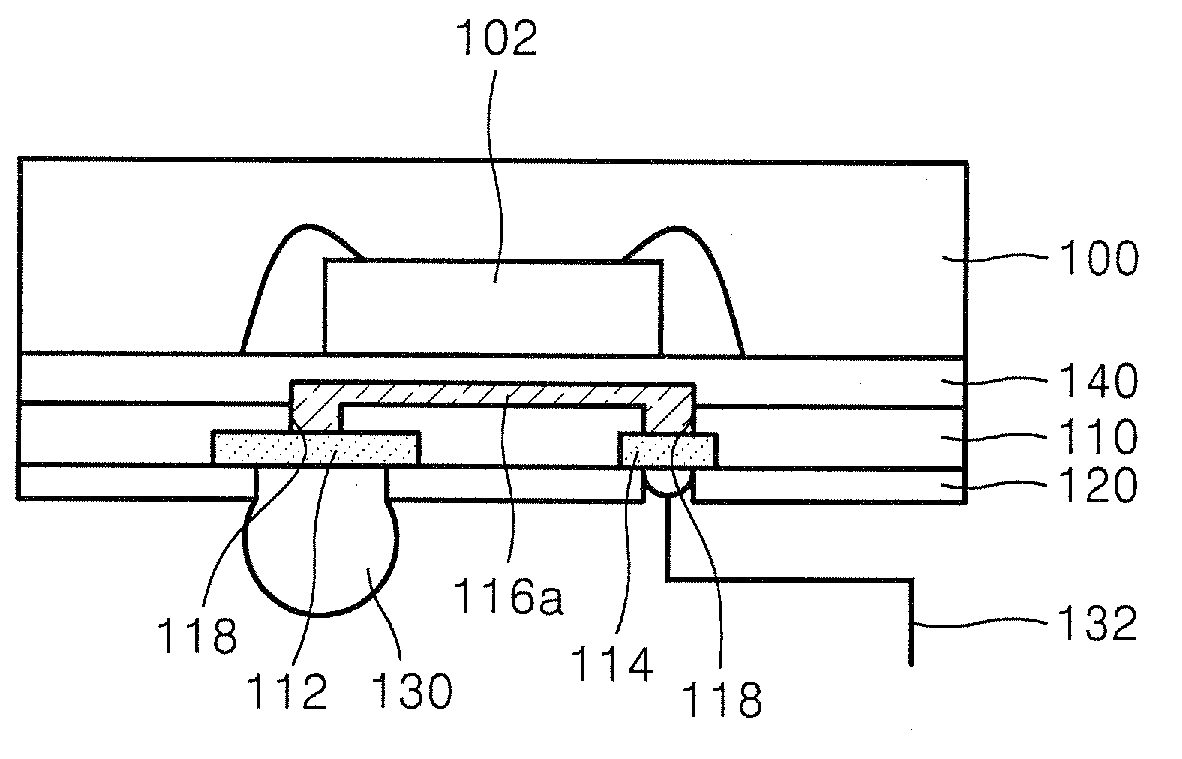
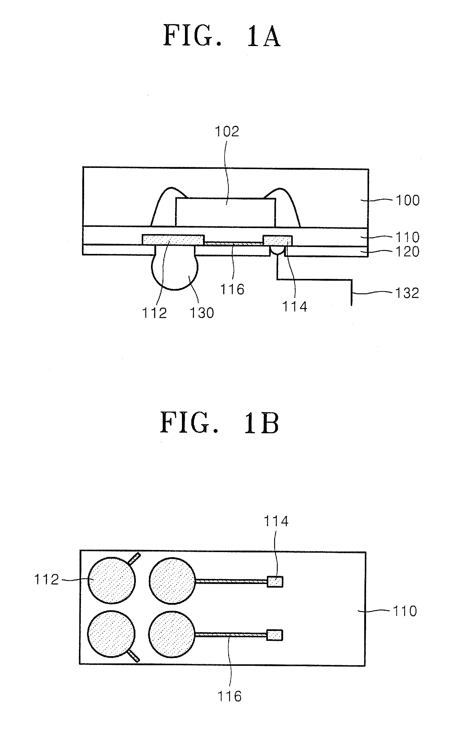
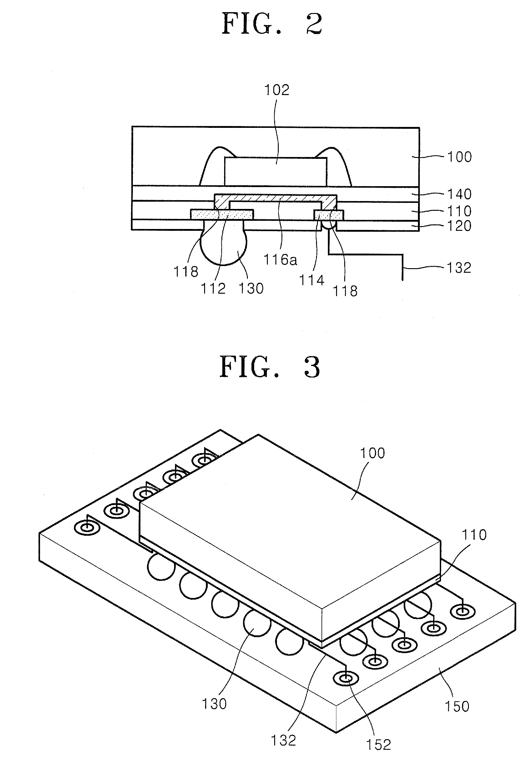
[0017]FIG. 1A is a cross-sectional view illustrating a semiconductor package according to an embodiment of the present invention, and FIG. 1B is a plan view illustrating a body having conductive pads disposed thereon. Here, the plan view illustrates a substrate.

[0018]Referring to FIGS. 1A and 1B, a semiconductor chip 102 is disposed on one side of the body 110, for example, a substrate, and a plurality of connection terminals, e.g., solder connection terminals 130 are disposed on the other side (hereinafter, rear side) of the substrate 110. One side of the substrate 110 including the semiconductor chip 102 may be referred to as a first surface and the other side may be referred to as a second surface. The plurality of solder connection terminals 130 are disposed individually. In other words, the solder connection terminals are not connected together. A plurality of conductive wires 132 externally protrude through a resist layer such as a photosensitive resist layer 120. The connecti...

second embodiment

[0031]FIG. 4 is a perspective view illustrating a semiconductor package according to another embodiment mounted on an external circuit board. The embodiment of the present invention shown in FIG. 4 is different from the embodiment of FIG. 1A in that the connection terminal, the wire, and the interconnection like FIG. 1A are formed in the semiconductor chip without use of the substrate.

[0032]Referring to FIG. 4, a connection terminal 130, a wire 132, and an interconnection 116 (FIG. 1A), which have been explained with reference to FIG. 1A, are formed in an active area of a flip chip 200. The active area is the portion where the flip chip 200 contacts an external circuit board 150. In the flip chip 200, the connection terminal 130 may be fabricated as a bump shape, using an electroplating method.

[0033]According to the embodiment of the present invention shown in FIG. 4, it is proposed that the connection terminal, the wire, and the interconnection, which are characteristic components ...


PUM


Abstract

A semiconductor package having a good joint to an external board, providing easy measurement control of the electrical characteristics of a semiconductor chip, and ensuring a sufficient number of input and output terminals, and a method of mounting the same are provided. The semiconductor package comprises a plurality of connection terminals aligned individually, and a plurality of conductive wires spaced from the connection terminals. The connection terminals and the wires are bonded to one side of a body, and an interconnection connecting at least one pair of the connection terminal and the wire is formed in the body.

Description

CROSS-REFERENCE TO RELATED PATENT APPLICATION[0001]This application claims priority from Korean Patent Application No. 10-2006-0054924, filed on Jun. 19, 2006, in the Korean Intellectual Property Office, the disclosure of which is incorporated herein in its entirety by reference.BACKGROUND[0002]1. Technical Field[0003]The present invention relates to a semiconductor package and a method of mounting the same, and more particularly, to a semiconductor package using interconnections electrically connecting a solder connection terminal such as a ball and a conductive wire, and a method of mounting the same.[0004]2. Description of the Related Art[0005]Normally, a sealed semiconductor chip is electrically connected to an external board using various methods. For example, the sealed chip can be attached to the external board using a solder joint, a wire, or a lead frame. However, these methods have many problems.[0006]The solder joint method may use relatively wide areas for interconnectio...

Claims


Application Information

Patent Timeline
IPC IPC(8): H01L23/48H01L21/44
CPCH01L22/34H01L23/49838H01L2224/48091H01L2224/48227H01L2924/15192H01L2924/15311H01L2924/19107H05K2201/10734H05K3/3415H05K3/3421H05K3/3436H05K2201/10659H01L2924/00014Y02P70/50H01L23/488
Inventor PARK, CHANG-YOUNG
Owner SAMSUNG ELECTRONICS CO LTD
Why Eureka
Try Eureka