

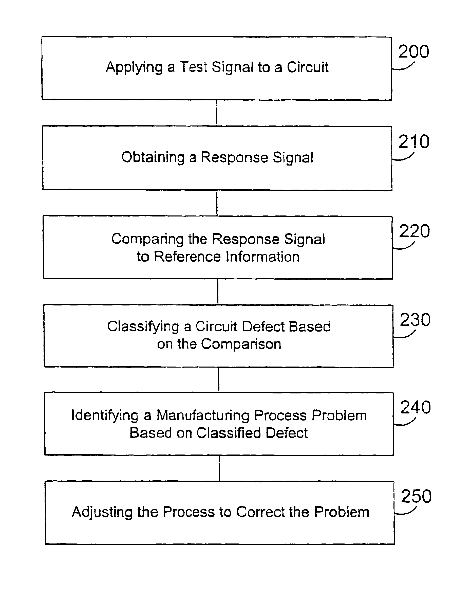
System and method for classifying defects in and identifying process problems for an electrical circuit
a technology of process problems and defect classification, applied in the field of testing electrical circuits, can solve problems such as inaccurate detection methods, inability to detect shorts between gates, and affecting the performance of transistor arrays, so as to improve the accuracy and efficiency of testing electronic circuits
- Summary
- Abstract
- Description
- Claims
- Application Information
AI Technical Summary
Benefits of technology
Problems solved by technology
Method used
Image

Examples
Embodiment Construction
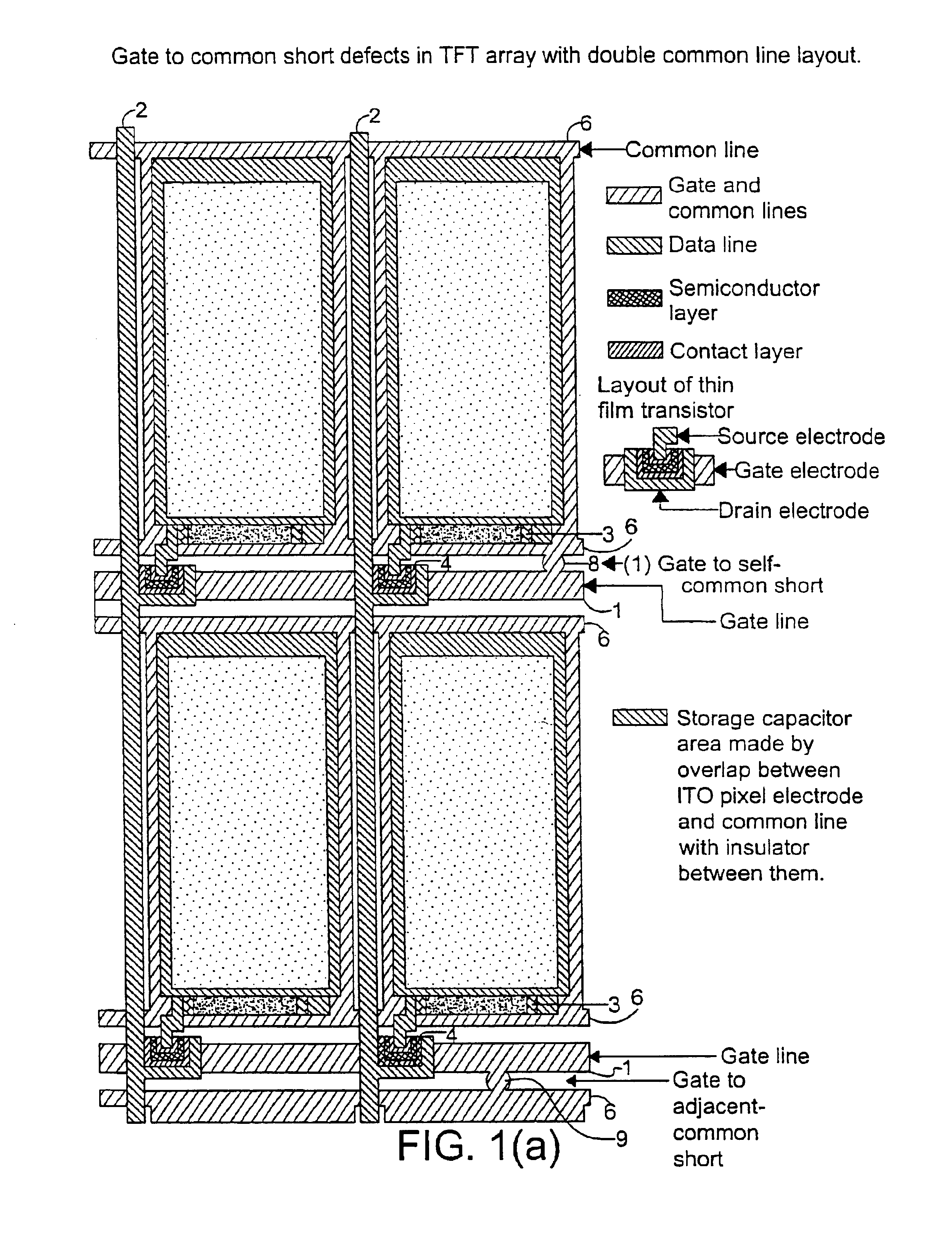
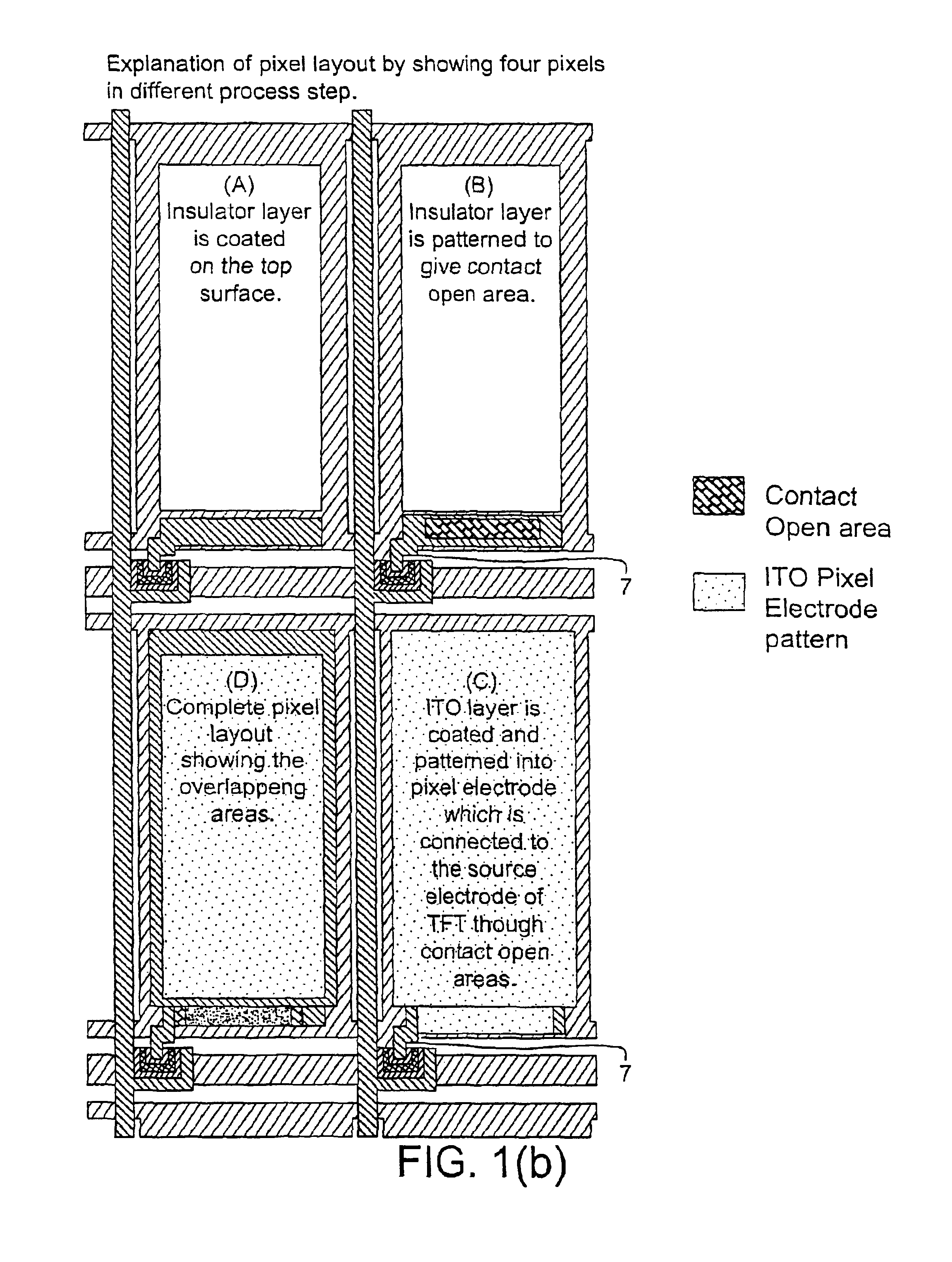
[0038]The present invention relates to a system and method for detecting a defect in an electronic circuit containing an array of transistors, and then accurately determining a location of the defect so that corrective action may be taken without disturbing other portions of the circuit that are properly functioning. The system and method are particularly well suited to detecting shorts that form between signal-carrying lines during the manufacturing process. The signal-carrying lines include but are not limited to gate lines and common lines, however the detection of defects of in other portions of the circuit is also possible. For example, the present invention may be implemented to detect at least the following types of opens and shorts: gate line open, common line open, local drain electrode open, local source electrode open, local gate electrode open, local gate-drain short, local gate-source short, local drain-source short, ITO pixel electrode-gate line short, ITO pixel electr...
PUM
 Abstract
Description
Claims
Application Information