System and method for detecting defects in a solar cell and repairing and characterizing a solar cell

a solar cell and defect detection technology, applied in the field of electronic circuit testing and repair, can solve the problems of low yield of solar cell manufacturing, low price of solar cell modules, and diminishing the number of working units, so as to improve the accuracy and efficiency of testing.

Inactive Publication Date: 2010-09-23
YIELDBOOST TECH
View PDF6 Cites 20 Cited by
  • Summary
  • Abstract
  • Description
  • Claims
  • Application Information

AI Technical Summary

Benefits of technology

[0009]An object of the present invention is to improve the accuracy and efficiency of testing and repairing electronic circuits including ones containing solar cells.

Problems solved by technology

A large barrier against the commercial expansion of the solar cell, however, is the high price of the solar-cell module, which may be caused by low yield of solar cell manufacturing.
During the manufacturing process of solar cell, defects may develop which, if left un-repaired, may diminish the number of working units and degrade the conversion efficiency of solar cell and / or reduce the manufacturing yield.

Method used


Image

  • System and method for detecting defects in a solar cell and repairing and characterizing a solar cell
  • System and method for detecting defects in a solar cell and repairing and characterizing a solar cell
  • System and method for detecting defects in a solar cell and repairing and characterizing a solar cell

Examples


Embodiment Construction

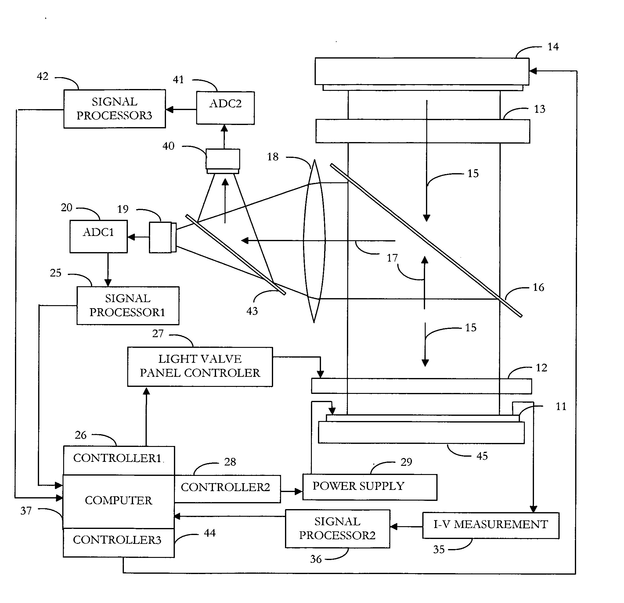
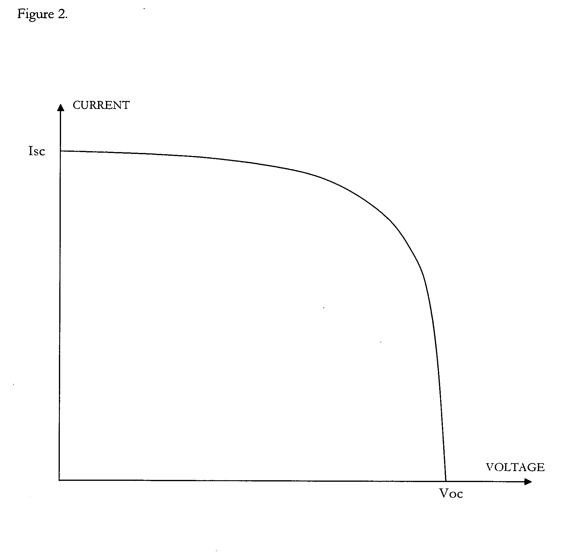
[0030]FIG. 1 is a block diagram of the test apparatus illustrating a structure to test and repair solar cells. A solar cell is tested after manufacturing process is completed to give functionality of current generation when the surface of solar cell receives light. In the FIG. 1 the solar cell under test (SUT) 11 may be tested in two modes, independently or in serial modes. The SUT can receive the optical input beam 15, which is generated by the optical energy source 14 and goes through the light valve panel (LVP) 12. The optical input beam 15, if necessary for collimation of light, may be expanded and collimated by the beam expander 13. If the SUT has no defect and works properly, then it generates photo-induced current and the I-V (current-voltage) measurement unit 35 measures the current-voltage characteristic as shown in FIG. 2, where Isc and Voc stand for a short circuit current and an open circuit voltage, respectively. FIG. 6 shows the equivalent circuit of a solar cell, wher...


PUM

PropertyMeasurementUnit
photocurrentaaaaaaaaaa
transmittanceaaaaaaaaaa
sizeaaaaaaaaaa

Abstract

A system and method for detecting a defect in a solar cell and repairing and characterizing a solar cell includes applying a test signal to the solar cell, monitoring the response of solar cell, detecting a defect associated with its location during the monitoring step, removing or isolating the defect from a solar cell and characterizing solar cell performance. The defect may be a short between the emitter and the base of solar cell. The system and method also detect a precise location of the defect based on the use of light valve panel (LVP), which can control the input beam to or output beam from the solar cell in terms of size, position, gray level, and wavelength of the transmitted light. The LVP may be realized in any one of a variety of ways. For example, the active matrix liquid crystal display (AMLCD) such as Thin Film Transistor driven LCD (TFT-LCD) may be used as the LVP.

Description

BACKGROUND OF THE INVENTION[0001]1. Field of the Invention[0002]This invention generally relates to testing and repairing electronic circuits, and more particularly to a system and method for detecting defects in a solar cell and repairing and characterizing the circuits which include one or more solar cells.[0003]2. Background of the Related Art[0004]Solar cell is one of the promising ones among the renewable energy resources as an alternative to fossil fuels. A large barrier against the commercial expansion of the solar cell, however, is the high price of the solar-cell module, which may be caused by low yield of solar cell manufacturing.[0005]During the manufacturing process of solar cell, defects may develop which, if left un-repaired, may diminish the number of working units and degrade the conversion efficiency of solar cell and / or reduce the manufacturing yield. These defects include electrical shorts between the top electrode, which is also called as the emitter, and the bot...

Claims


Application Information

Patent Timeline
Patent Type & Authority Applications(United States)
IPC IPC(8): H01L31/18G01R31/308G01N27/00
CPCG01R31/308Y10T29/41H02S50/10H01L31/18Y02E10/50
Inventor CHUNG, KYO YOUNG
Owner YIELDBOOST TECH
Why Eureka
Try Eureka