Semiconductor structure implementing low-K dielectric materials and supporting stubs

a dielectric material and semiconductor technology, applied in semiconductor devices, semiconductor/solid-state device details, electrical apparatus, etc., can solve the problems of poor mechanical strength of porous dielectric materials, low possibility of cross-metallization line signal interference, and difficult to replace aluminum with copper. , to achieve the effect of reducing the capacitance of inter-metal dielectrics and fast integrated circuit devices

Inactive Publication Date: 2006-01-10
LAM RES CORP
View PDF13 Cites 22 Cited by
  • Summary
  • Abstract
  • Description
  • Claims
  • Application Information

AI Technical Summary

Benefits of technology

[0014]The advantages of the present invention are numerous. Most notably, even though the semiconductor structure of the present invention ultimately implements air or low-K dielectric materials as a dielectric, the semiconductor structure of the present invention withstands the structural stresses and pressures that occur during CMP and other operations. In this manner, while inter-metal dielectric capacitance is minimized and faster integrated circuit devices are produced, the shortcomings associated with implementing air or low-K dielectric materials in semiconductor fabrication processes are substantially eliminated.

Problems solved by technology

However, replacing aluminum with copper has been problematic, as it mandates a fundamental change in the metal interconnect formation.
Second, low-K dielectric materials reduce cross-talk noise, since the lower is the dielectric constant of a dielectric, the lower is the possibility of cross-metallization line signal interference.
However, the poor mechanical strength of such porous dielectric materials as well as the current state of the semiconductor fabrication technology hinder their implementation in the semiconductor fabrication process.
Particularly, the poor mechanical strength of low-K dielectric materials is problematic during the chemical mechanical planarization (CMP) operation performed on copper metallization lines.
However, performing a CMP operation on a semiconductor device having porous low-K dielectric material is complicated as the application of the substrate surface onto the polishing pad may cause regions of the semiconductor structure to collapse or crack, thus hindering performance or requiring that the fabricated semiconductor wafer be discarded.
As can be appreciated, when these problems are introduced during semiconductor fabrication processes, the yield of good chips can dramatically decrease, in addition to reducing wafer throughput.

Method used


Image

  • Semiconductor structure implementing low-K dielectric materials and supporting stubs
  • Semiconductor structure implementing low-K dielectric materials and supporting stubs
  • Semiconductor structure implementing low-K dielectric materials and supporting stubs

Examples


Embodiment Construction

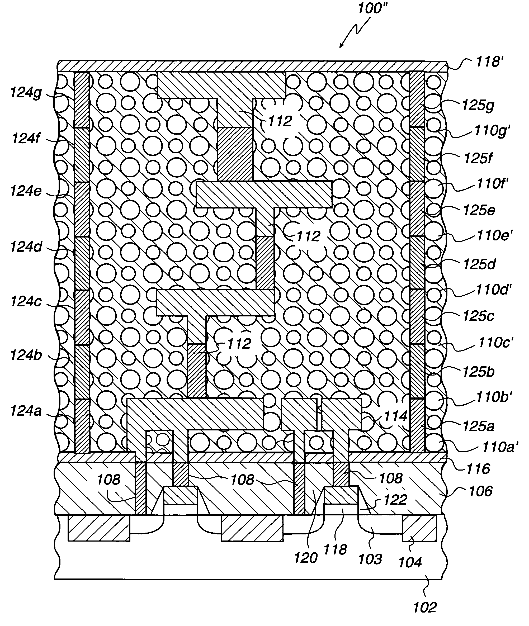
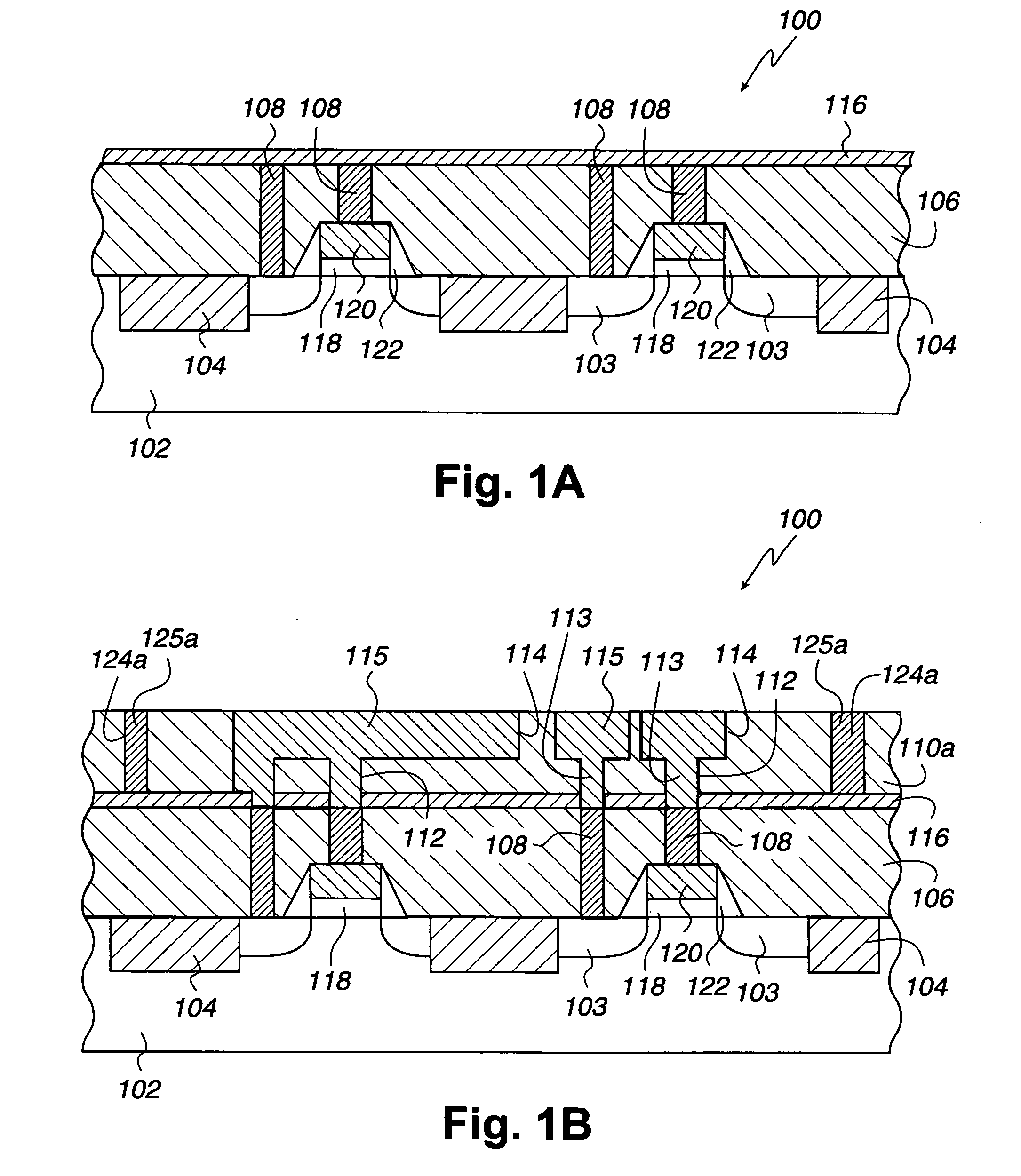
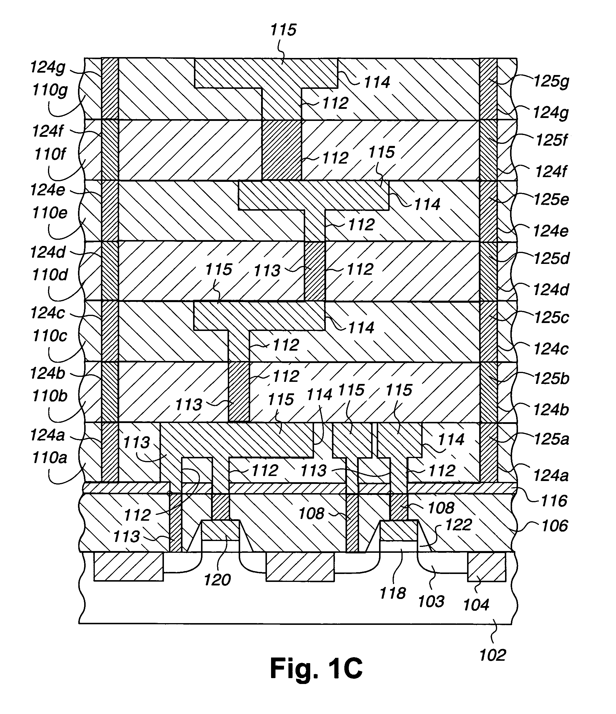
[0027]Embodiments for making semiconductor structures that optimize semiconductor performance by minimizing inter-metal dielectric capacitance are described. In one preferred embodiment, a sacrificial material is used during the fabrication of each layer of copper interconnects and then is etched out and replaced with an insulator having a low dielectric constant. In another embodiment, a plurality of stubs are formed in the sacrificial layer, thus creating nearly continuous supporting columns for when the sacrificial layer is etched away. In preferred implementations, the substantially continuous supporting columns of stubs are configured to extend from the passivation layer to a passivation-capping layer, thus forming a semiconductor structure having high structural integrity with reduced capacitance related delay. In a preferred embodiment, the plurality of stubs are constructed from copper. In another embodiment, the sacrificial layer is a dielectric and the low-K dielectric mat...


PUM


Abstract

A semiconductor device is provided. The semiconductor device includes a substrate having transistor devices and a plurality of copper interconnect metallization lines and conductive vias. The plurality of copper interconnect metallization lines and conductive vias are defined in each of a plurality of interconnect levels of the semiconductor device such that the plurality of copper interconnect metallization lines and conductive vias are isolated from each other by an air dielectric. The semiconductor device further includes a plurality of supporting stubs each of which is configured to form a supporting column that extends through the plurality of interconnect levels of the semiconductor device.

Description

BACKGROUND OF THE INVENTION[0001]1. Field of the Invention[0002]The present invention relates generally to semiconductor device fabrication technology and techniques for improving the performance of semiconductor devices. Specifically, the present invention relates to implementing sacrificial materials to enhance the performance of semiconductor devices.[0003]2. Description of the Related Art[0004]As is well known, the semiconductor industry is moving toward implementing larger substrates having higher density with devices having smaller features. To achieve this task, millions of transistors are connected through multiple layers of interconnect metallization lines, insulating dielectric layers, and conductive via structures and are fabricated on a wafer substrate. Originally, metallization lines and vias were predominantly formed from aluminum, as it is relatively inexpensive, easy to etch, and has relatively low resistivity, while insulators were made predominantly from silicon di...

Claims


Application Information

Patent Timeline
Patent Type & Authority Patents(United States)
IPC IPC(8): H01L23/48H01L29/00H01L21/768H01L23/522H01L23/532
CPCH01L21/7682H01L23/5222H01L23/53228H01L23/5329H01L2924/0002H01L2924/00H01L2221/1047H01L21/768
Inventor GOTKIS, YEHIELWEI, DAVIDKISTLER, RODNEY
Owner LAM RES CORP
Why Eureka
Try Eureka