Self-assembled nanometer conductive bumps and method for fabricating

a self-assembled, nanometer technology, applied in the direction of conductive pattern reinforcement, nanoinformatics, printed element electric connection formation, etc., can solve the problems of damage to the devices formed on the wafer, the conventional cvd method for forming carbon nanotubes is not suitable for forming conductive bumps on the wafer

Inactive Publication Date: 2006-01-24
IND TECH RES INST
View PDF6 Cites 89 Cited by
  • Summary
  • Abstract
  • Description
  • Claims
  • Application Information

AI Technical Summary

Problems solved by technology

As a result, requirements for the packaging and interconnection of devices become more stringent.
However, the lowest possible operating temperature for the chemical vapor deposition process is about 700° C., which may damage the devices formed on the wafer.
The conventional CVD method for forming carbon nanotubes is therefore not suitable for forming conductive bumps on wafers.
Other reaction methods utilizing a direct interaction between metal-carbide which also requires high temperature and is similarly undesirable.

Method used


Image

  • Self-assembled nanometer conductive bumps and method for fabricating
  • Self-assembled nanometer conductive bumps and method for fabricating
  • Self-assembled nanometer conductive bumps and method for fabricating

Examples


Embodiment Construction

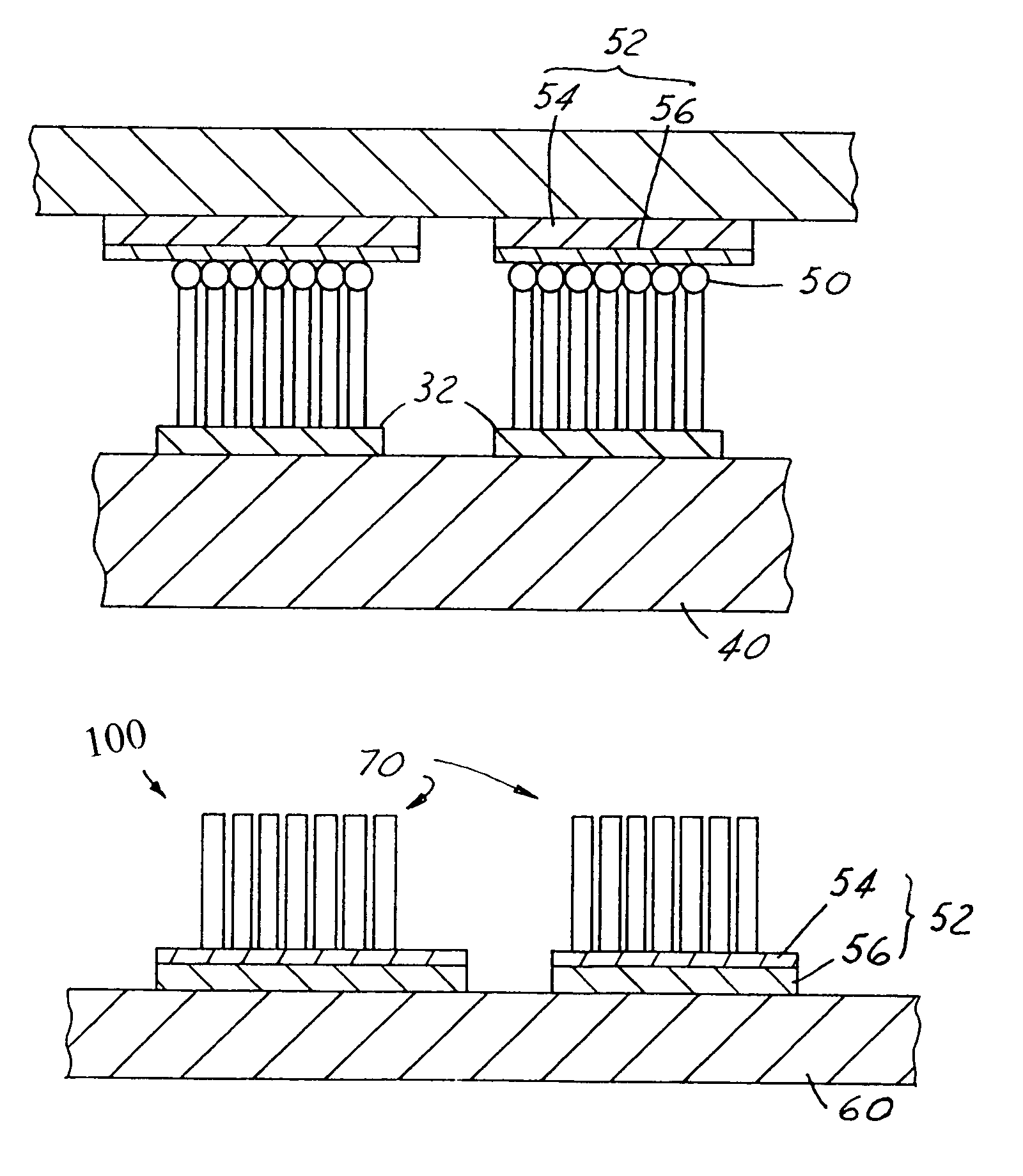
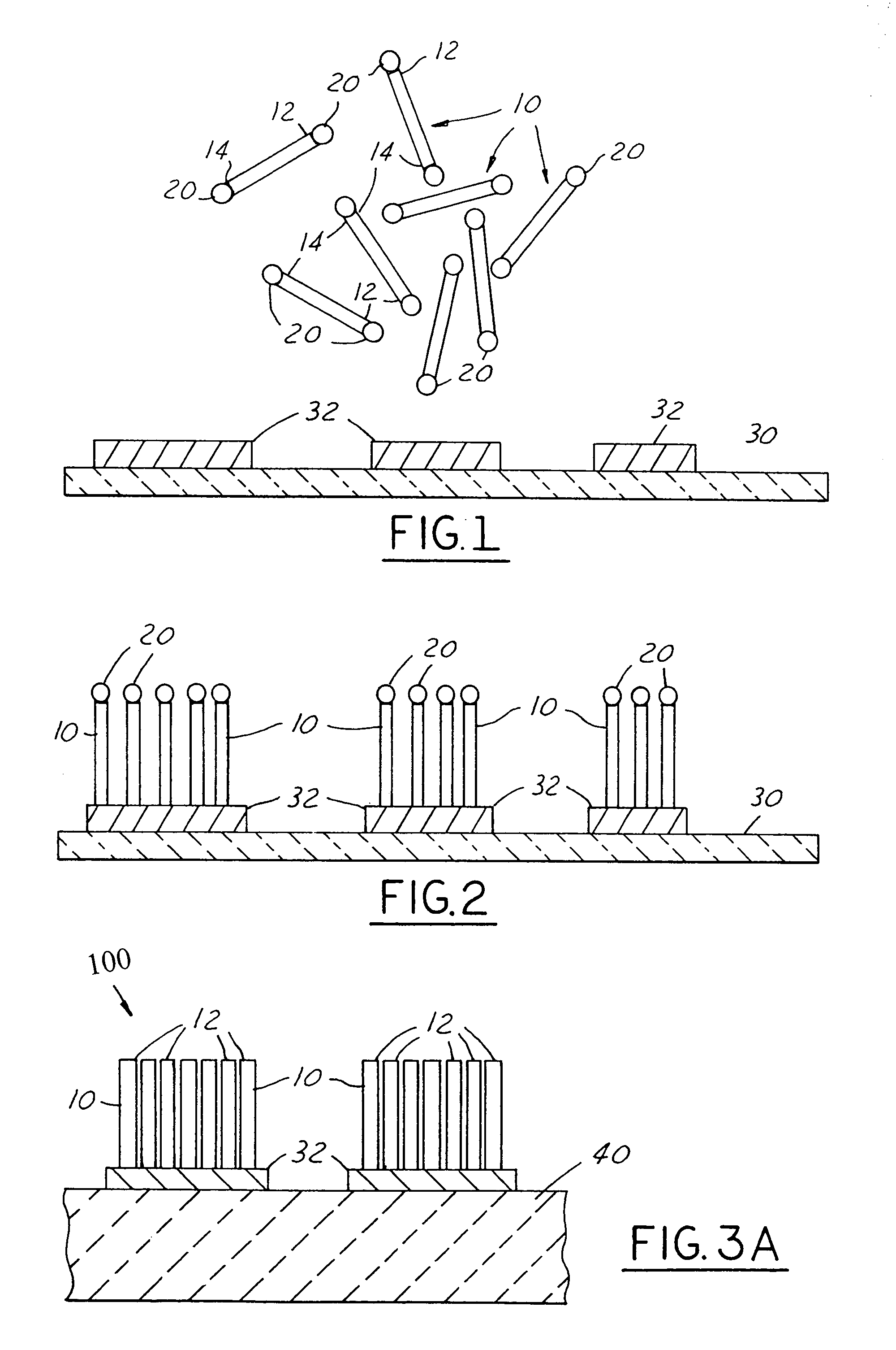
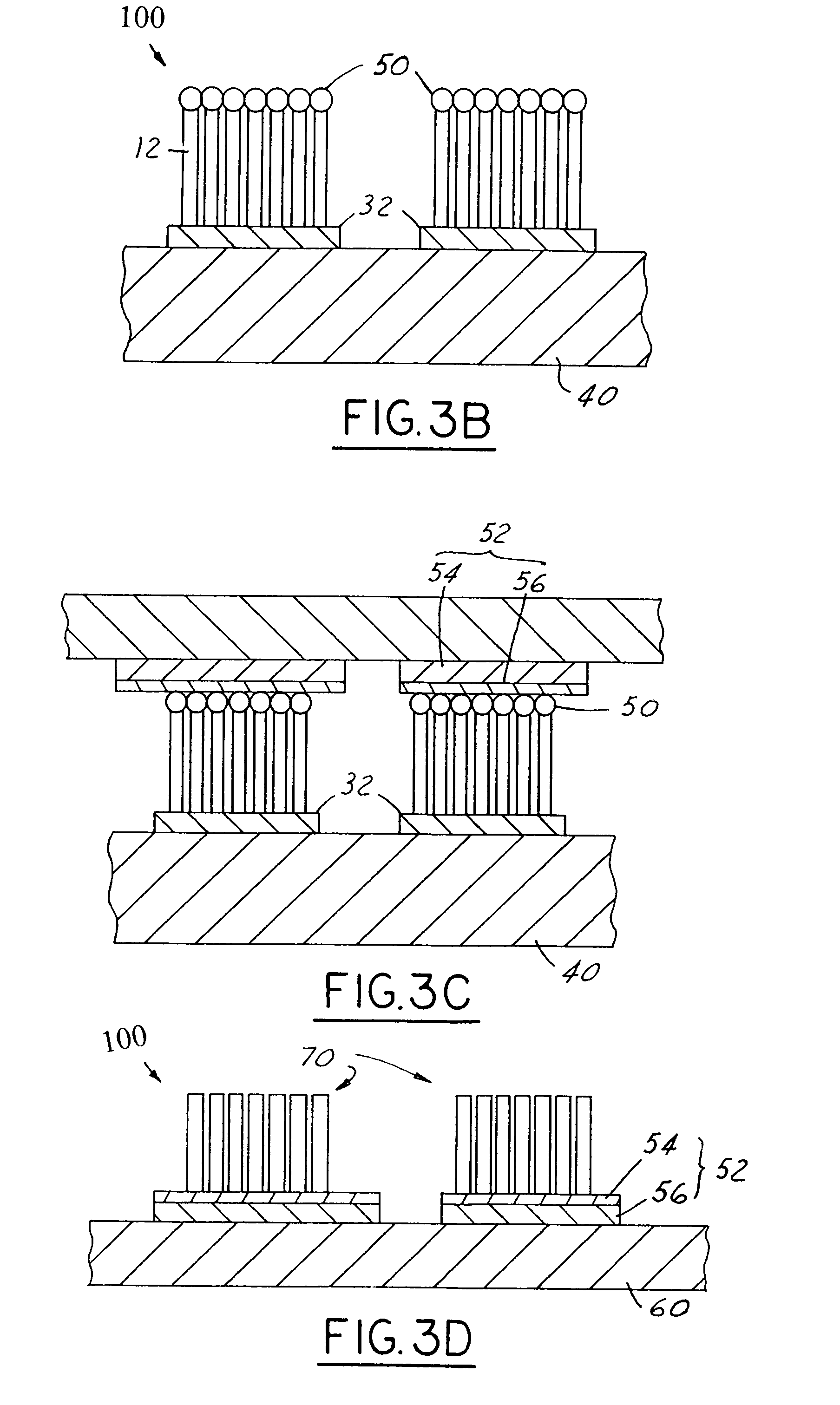
[0024]The present invention discloses a self-assembly method for fabricating nanometer conductive bumps and the carbon nanotube conductive bumps fabricated. The carbon nanotube conductive bumps can be used to provide electrical connection between a semiconductor device and a substrate. The carbon nanotubes are self-assembled onto metal pads situated on a substrate by first attaching chemically functional groups to the ends of the carbon nanotubes.

[0025]To achieve the present invention, the two ends of the carbon nanotubes are attached chemically functional groups and then, due to a chemical affinity existed between the functional groups and the metal pad, bond the carbon nanotubes to the metal pads. The term “self-assemble” is thus used to describe the fact that the carbon nanotubes are able to assemble themselves onto the metal pad by the strong chemical affinity existed between the chemically functional groups and the metal pad. To facilitate the present invention novel method, di...


PUM

PropertyMeasurementUnit
distanceaaaaaaaaaa
distanceaaaaaaaaaa
lengthaaaaaaaaaa

Abstract

A self-assembled nanometer conductive bump and a method for fabricating the bump. In the method, a multiplicity of carbon nanotubes that are coated at two ends with chemically functional groups is first provided. A substrate that is equipped with at least one bond pad on a surface is then positioned juxtaposed to the carbon nanotubes for forming a bond between the carbon nanotubes and the metal pads facilitated by a chemical affinity existed between the functional groups and the metal pad.

Description

FIELD OF THE INVENTION[0001]The present invention generally relates to nanometer conductive bumps and a method for fabricating the bumps. More particularly, the present invention is related to nanometer conductive bumps formed by carbon nanotubes and a method for fabricating the bumps.BACKGROUND OF THE INVENTION[0002]In the development of modern semiconductor devices, the requirements for ever increasing device density and ever decreasing device dimensions are frequently encountered. As a result, requirements for the packaging and interconnection of devices become more stringent. The technology of flip-chip bonding or flip-chip direct chip attachment (DCA) have been developed to satisfy such stringent requirements in semiconductor packaging.[0003]In the technology of flip-chip bonding, a multiplicity of bumps is normally formed on the active surface of a wafer. The multiplicity of bumps is formed on top of a multiplicity of input / output bond pads in order to provide the function for...

Claims


Application Information

Patent Timeline
Patent Type & Authority Patents(United States)
IPC IPC(8): H01L21/44H01L21/60H01L23/485H01L23/532H05K3/24H05K3/40
CPCB82Y10/00H01L24/11H05K3/249H05K3/4007H01L24/13H01L2224/1133H01L2224/13099H01L2924/01016H01L2924/01029H01L2924/01046H01L2924/01047H01L2924/01078H01L2924/01079H01L2924/01082H01L2924/01322H05K3/06H05K2201/026H01L2924/01006H01L2924/01033H01L2924/014Y10S977/882H01L2224/13193H01L23/53276H01L2924/0001H01L2924/00014H01L2924/12042H01L2224/0508H01L2224/05573H01L2224/05568H01L2224/05023H01L2224/05001H01L2224/05111H01L2224/05639H01L2224/05644H01L2224/05647H01L2224/05664H01L2224/05669H01L24/05H01L2924/00
Inventor UANG, RUOH-HUEYCHEN, YU-HUA
Owner IND TECH RES INST
Why Eureka
Try Eureka