Chemical vapor deposition precursors for deposition of tantalum-based materials

a technology of precursors and vapor deposition, which is applied in the direction of organic chemistry, group 5/15 element organic compounds, electric/magnetic/electromagnetic heating, etc., can solve the problems of unsatisfactory use of tantalum-based materials as diffusion barriers for copper metallization, and the suitability of pvd processes for deposition

Inactive Publication Date: 2006-01-24
ENTEGRIS INC
View PDF2 Cites 28 Cited by
  • Summary
  • Abstract
  • Description
  • Claims
  • Application Information

AI Technical Summary

Benefits of technology

[0003]Although the use of physical vapor deposition (PVD) is commonly employed for forming Ta, TaN and TaSiN thin film diffusion barrier layers, there are substantial and unresolved issues concerning the suitability of PVD processes for deposition at dimensions below 0.13 μm, as is required in the fabrication of future high performance microelectronic devices.

Problems solved by technology

Although the use of physical vapor deposition (PVD) is commonly employed for forming Ta, TaN and TaSiN thin film diffusion barrier layers, there are substantial and unresolved issues concerning the suitability of PVD processes for deposition at dimensions below 0.13 μm, as is required in the fabrication of future high performance microelectronic devices.
Considering chemical vapor deposition as a potential deposition technique, currently available organometallic tantalum precursors suffer from the incorporation of high levels of carbon, nitrogen and oxygen in the deposited tantalum film, which render the deposited tantalum-based material unsatisfactory for use as a diffusion barrier for copper metallization.

Method used


Image

  • Chemical vapor deposition precursors for deposition of tantalum-based materials
  • Chemical vapor deposition precursors for deposition of tantalum-based materials
  • Chemical vapor deposition precursors for deposition of tantalum-based materials

Examples


example 1

Synthesis of TMSCp2TaH3

[0046]To 5.6 grams of freshly distilled trimethylsilylcyclopentadiene (TMSCp) in tetrahydrofuran (THF) was added 10% excess solution of BuLi in hexane. Upon completion of addition the mixture was stirred for 12 hours. The color of the reaction solution at the completion of the reaction was yellow. No solid formation was observed, due to the high solubility of the material in THF. To the freshly prepared solution of TMSCpLi (40 mmol) in THF and NaBH4 (1.125 grams) was added slowly 3.5 grams of TaCl5. On completion of addition, the mixture was refluxed for 4 hours following which 0.54 milliliter of degassed distilled water was added very slowly. After completion of the addition, the mixture was refluxed for an additional 5 minutes following which the volatiles were removed under vacuum. The compound was extracted with pentane and stored in the freezer. Brown crystals of TMSCp2TaH3 were obtained and washing these crystals with pentane gave very pure white crysta...

example 2

Synthesis of Cp2TaH2(t-Bu)SiH2

[0052]To 0.5 gram of Cp2TaH3 in toluene was added 0.35 gram of t-BuSiH3 in toluene. The reaction mixture was heated in a quartz reaction vessel at 135° C. for 6 days with three freeze-pump-thaw cycles each day. The solution was bright yellow in color. The solution was filtered and pumped to dryness. Pumping the solvent resulted in crystalline white material. 96% yield was achieved.

[0053]Characterization

[0054]1H NMR (C6D6): −4.73 (s, 2H, TaH2), 1.37 (s, 9H, t-Bu), 4.57 (s, 10H, Cp), 4.81 (s, 2H, SiH2). 13C NMR (C6D6): 30.42 (t-Bu), 85.81 (Cp).

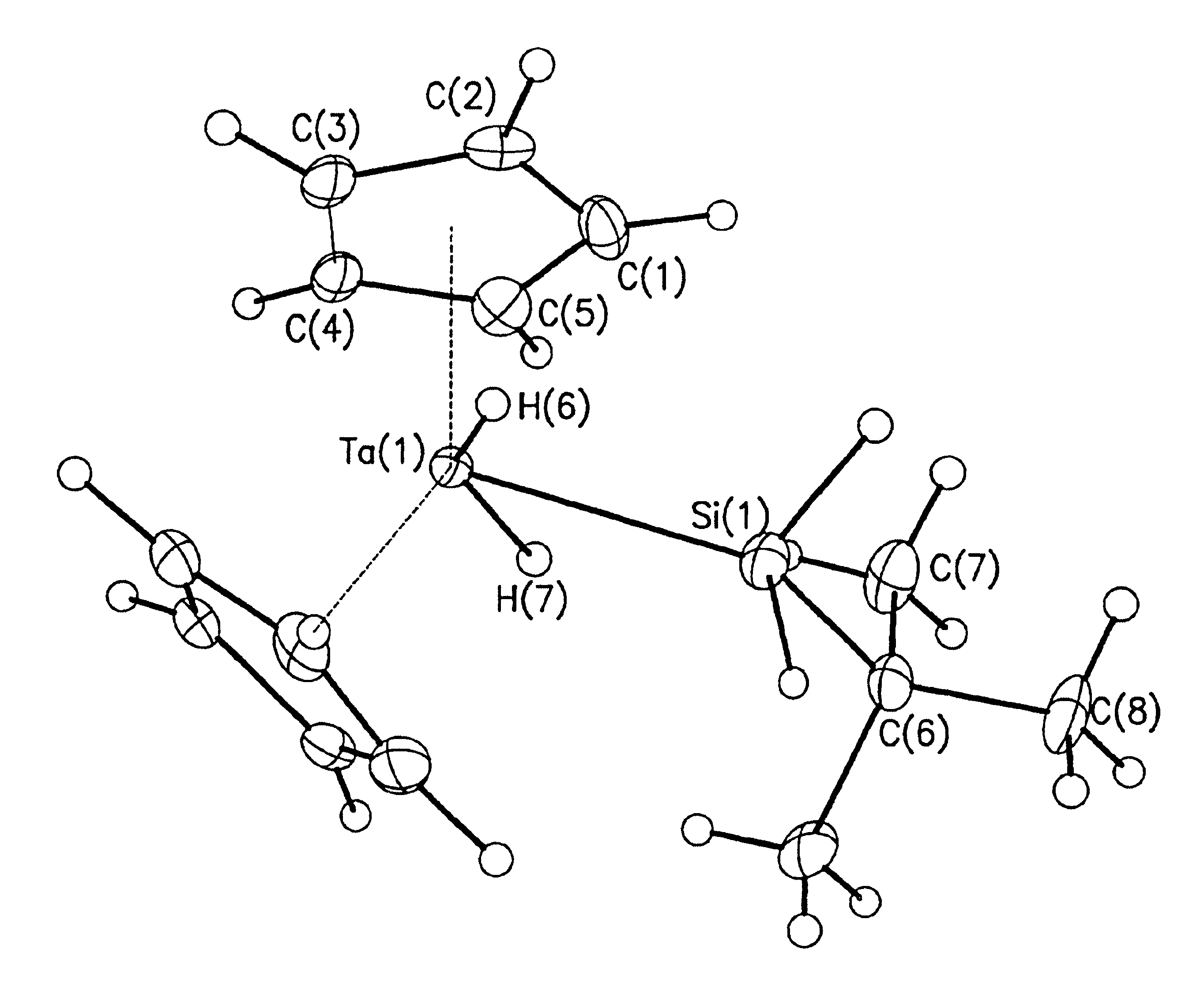
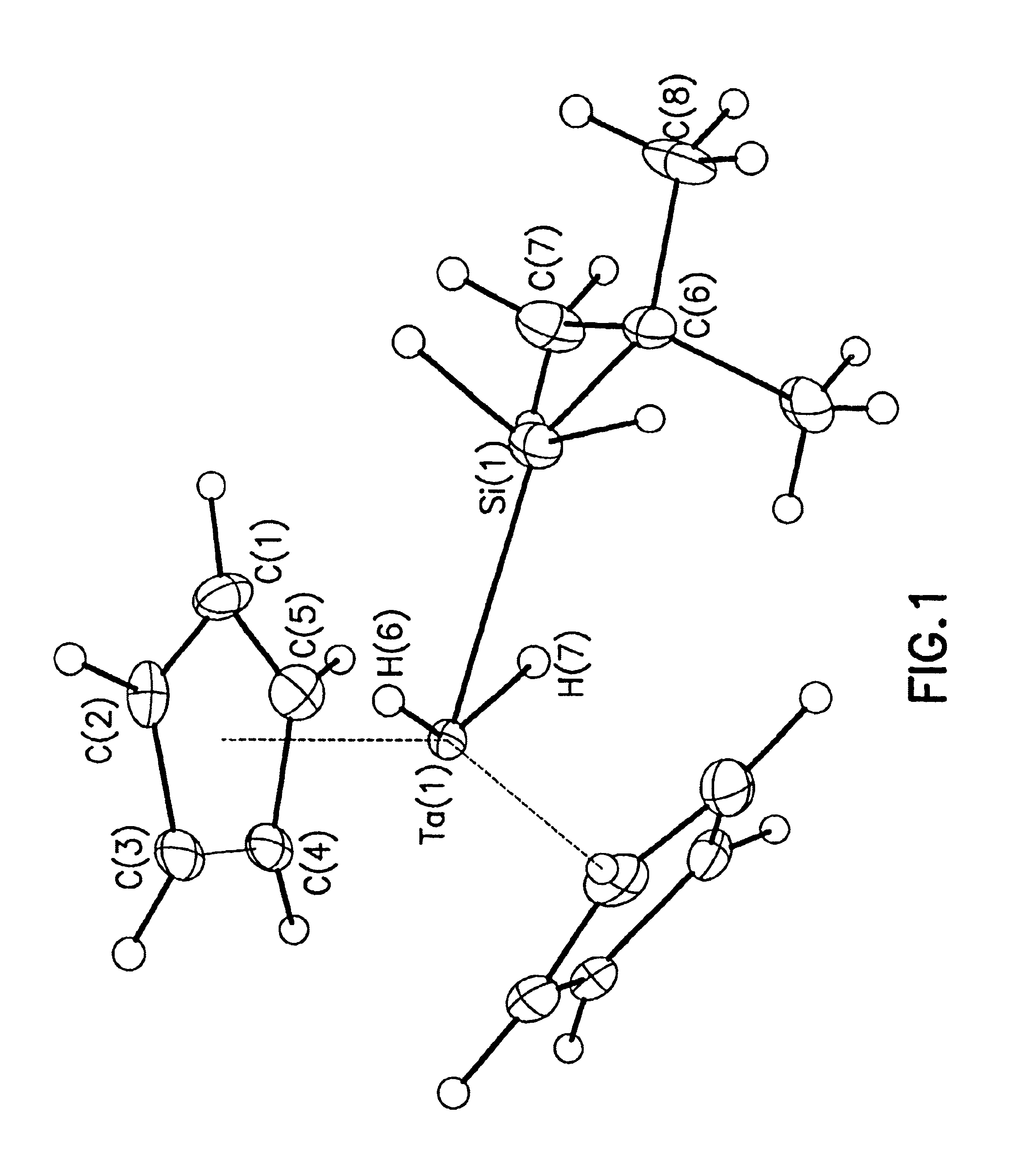
[0055]Crystal Structure

[0056]The crystal structure of the product Ta / Si compound, Cp2TaH2(t-Bu)SiH2, is shown in the ORTEP diagram of FIG. 1 hereof.

[0057]The Ta / Si compound of this example is usefully employed to form silicon-doped tantalum material layers as barrier layers on substrates in the fabrication of microelectronic devices and device precursor structures.


PUM

PropertyMeasurementUnit
melting pointaaaaaaaaaa
semiconductoraaaaaaaaaa
line dimensionaaaaaaaaaa

Abstract

Tantalum precursors suitable for chemical vapor deposition of tantalum-containing material, e.g., tantalum, TaN, TaSiN, etc., on substrates. The tantalum precursors are substituted cyclopentadienyl tantalum compounds. In one aspect of the invention, such compounds are silylated to constitute tantalum / silicon source reagents. The precursors of the invention are advantageously employed in semiconductor manufacturing applications to form diffusion barriers in connection with copper metallization of the semiconductor device structure.

Description

FIELD OF THE INVENTION[0001]The present invention relates to the deposition of tantalum-based materials, and to precursor compositions having utility for chemical vapor deposition of such materials on substrates, e.g., in the manufacture of semiconductor products.DESCRIPTION OF THE RELATED ART[0002]The ability to deposit conformal tantalum-based diffusion barriers is critical to the widespread adoption of copper metallization technology in semiconductor manufacturing operations.[0003]Although the use of physical vapor deposition (PVD) is commonly employed for forming Ta, TaN and TaSiN thin film diffusion barrier layers, there are substantial and unresolved issues concerning the suitability of PVD processes for deposition at dimensions below 0.13 μm, as is required in the fabrication of future high performance microelectronic devices.[0004]Considering chemical vapor deposition as a potential deposition technique, currently available organometallic tantalum precursors suffer from the ...

Claims


Application Information

Patent Timeline
Patent Type & Authority Patents(United States)
IPC IPC(8): C07F9/00B05D1/02H01L21/44C23C14/26C07F17/00C23C16/18C23C16/34
CPCC07F17/00C23C16/34C23C16/18C23C16/00
Inventor KAMEPALLI, SMURUTHIBAUM, THOMAS H.
Owner ENTEGRIS INC
Why Eureka
Try Eureka