[0065]Hereinafter, a receiver in a CDMA system of the present invention will be described below in detail with reference to the attached drawings.
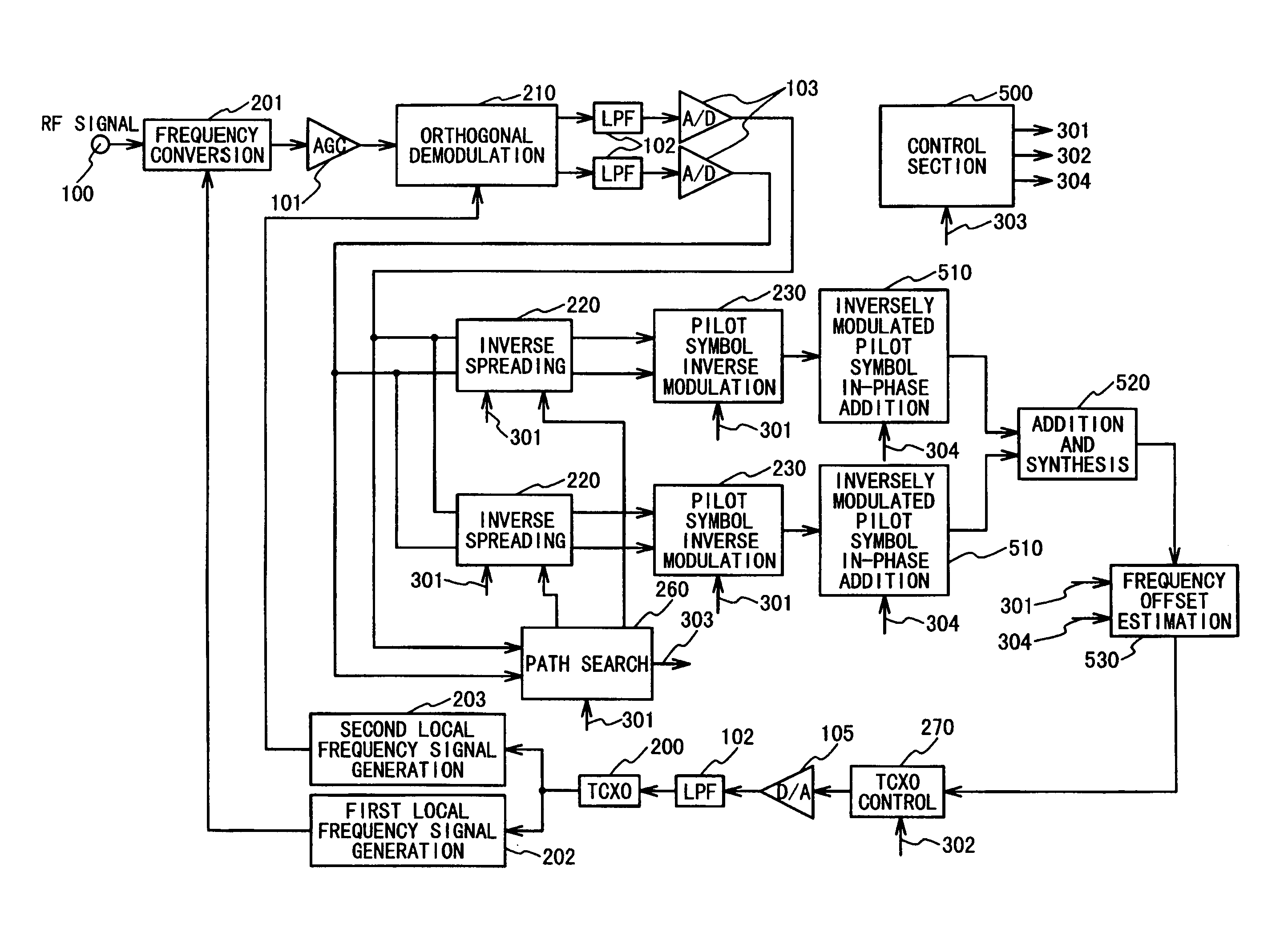
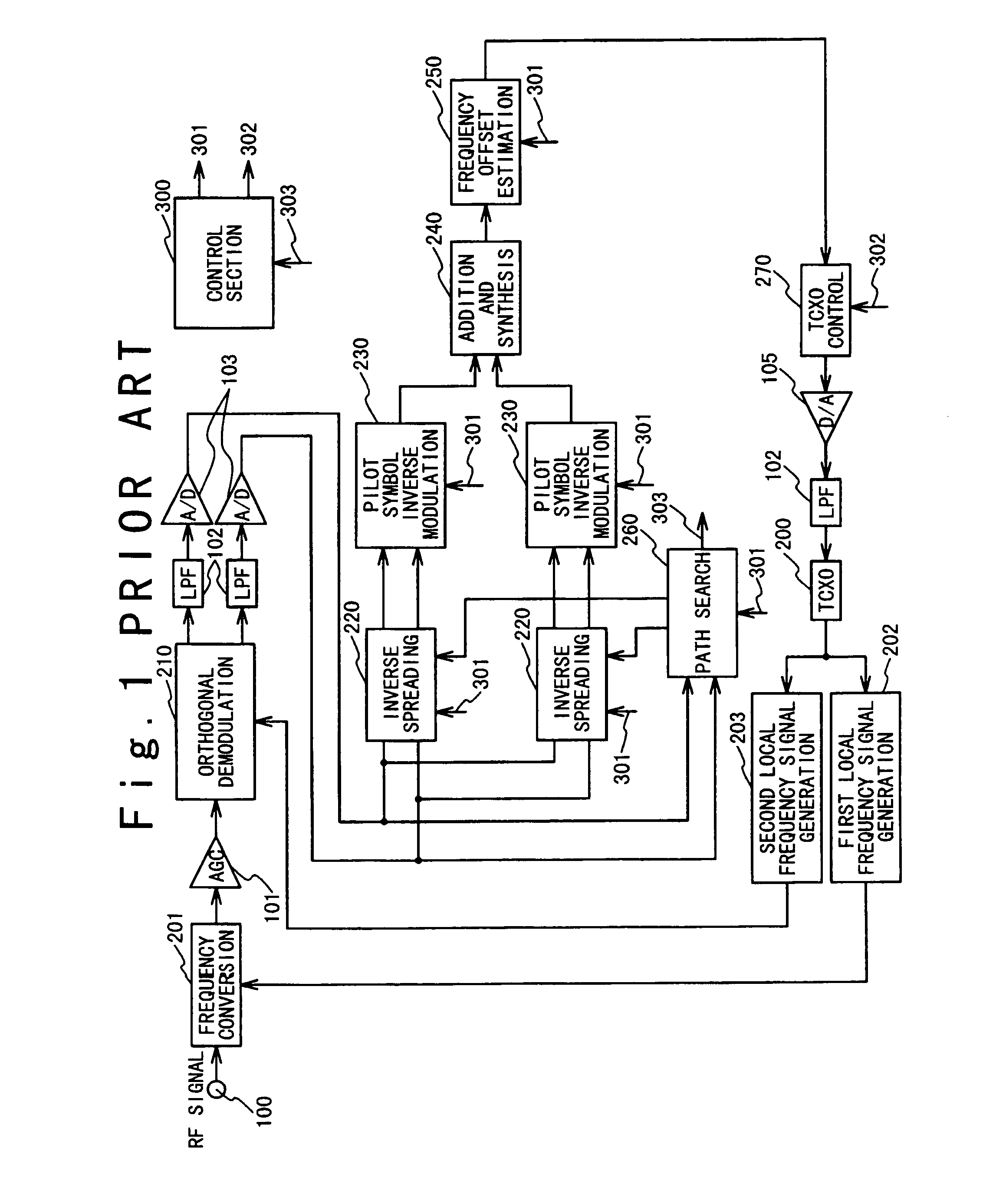
[0066]FIG. 5 is a block diagram showing the structure of the receiver in the CDMA system according to an embodiment of the present invention. In this embodiment a structure relating to an inverse demodulation pilot symbol in-phase adders 510, an addition synthesizer 520, a frequency offset estimator 530, and a controller 500 is added or modified compared with the conventional system shown in FIG. 1. The other components are substantially identical to those of the conventional apparatus shown in FIG. 1. The blocks denoted by the same reference numerals as those shown in FIG. 1 are identical to those shown in FIG. 5 in the function and operation.
[0067]Referring to FIG. 1, an RF (radio frequency) signal, i.e., a high frequency signal from a transmitter received by an antenna is introduced to a frequency converter 201 via an input terminal 100. The frequency converter 201 receives a first local frequency signal from the first local frequency generator 202. A first local frequency signal is obtained by offsetting the frequency of a carrier signal from the transmitter by an IF frequency. The frequency converter 201 as a mixer converts the RF signal into an IF (intermediate frequency) signal in accordance with the first local frequency signal. The IF signal is then adjusted to a predetermined signal level by an AGC unit 101 and transferred to an orthogonal demodulator 210. A second local frequency signal having an IF frequency is supplied from a second local frequency generator 203 to an orthogonal demodulator 210. In response to the second local frequency signal, the orthogonal demodulator 210 converts the IF signal into a baseband signal which has a component I along an in-phase axis and a component Q along an orthogonal axis. It is now assumed that QPSK modulation is employed. The in-phase component and the orthogonal component of the orthogonally demodulated signal are passed through two LPF units 202, respectively, and fed to A/D converters 103 which converts into their digital signals. Then, the converted digital signals are transferred to inversely spreading units 220 and a path searching unit 260. The path searching unit 260 determines a delay profile from the digital signals supplied from the A/D converters 103 to determine the timing for inverse spreading used in the inversely spreading units 220. The intervals for which the delay profile is calculated and the averaged length of the intervals are determined based on an instruction 301 from the controller 300. The path searching unit 260 outputs an inverse spreading timing to the inversely spreading units 220 based on the determined delay profile. Also, the path searching unit 260 determines how many effective multi-paths are present in the received digital signals and delivers its result 303 to the controller 300.
[0068]The inversely spreading units 220 receives a control signal 301 from the controller 300. The control signal 301 includes parameter data 301 such as a spreading code and symbol rate of the channel and boundary data of a pilot symbol interval. The inversely spreading units 220 inversely spread the digital signals received from the A/D converters 103 into symbol signals based on the inverse spreading timing received from the path searching unit 260 and the control signal 301. The symbol signals are transferred to pilot symbol inverse demodulators 230. In this conventional example, it is assumed that a pilot symbol signal and a data symbol signal are time-multiplexed in the symbol signal to have a QPSK transmission format, as illustrated in FIG. 2A. A pilot symbol interval is inserted before a data symbol interval for every slot period having a predetermined interval called “a slot”. A pilot symbol pattern in the pilot symbol interval in each slot period is variable. In this case, the symbol rate can be made variable by changing the spreading rate under a constant chip rate as shown in FIG. 2D. More specifically, the symbol interval in the symbol rate of 2*Fs is decreased to a half of the symbol interval in the symbol rate of Fs, as shown in FIGS. 2B and 2C.
[0069]It should be noted that the pilot symbol interval remains unchanged in the length when the symbol rate is varied in FIGS. 2B and 2C. However, there generally is no such a limitation. The pilot symbol interval length may be varied depending on the symbol rate Fs.
[0070]The controller 500 shown in FIG. 5 receives the number of effective paths 303 from the path searching unit 260. The controller 500 generates a reception channel data such as the spreading code, the symbol rate, and the number of pilot symbols or pilot symbol interval. Also, the controller 500 generates various parameters for frequency offset estimation such as the number of data for phase difference average summation and angle/frequency offset conversion factors. In addition, the controller 500 generates temperature compensated crystal oscillator (TCXO) control data such as a conversion table between frequency offset and TCXO control voltage and the validation or invalidation of an updating operation of frequency offset. In this case, the controller 500 supplies the reception channel data by the control signal 301 to the path searching unit 260, the inverse spreading units 220, the pilot symbol inverse modulators 230 and a frequency offset estimator 530. Also, the controller 500 supplies the parameters for frequency offset estimation and a part of the TCXO control data such as the validation or invalidation of the updating operation of frequency offset to an inverse modulation pilot symbol in-phase adders 510 and the frequency offset estimator 530 by a control signal 304. The controller 500 supplies a value of the conversion table between frequency offset and TCXO control voltage to the TCXO controller 270 by a control signal 502.
[0071]FIG. 6 illustrates the structure of the pilot symbol inverse demodulator 230 and the inversely demodulated pilot symbol in-phase adder 510. In the pilot symbol inverse demodulator 230, a controller 239 generates a generation control signal to the reference pilot symbol generator 232 in response to the control signal 301 from the controller 500. The reference pilot symbol generator 232 generates a pilot symbol pattern for a symbol rate and a concerned slot in response to the generation control signal to output to a pilot symbol inverse demodulator 233. The pilot symbol pattern for the symbol rate and the concerned slot necessary for the inverse demodulation. Thus, the length of the pilot symbol interval is determined based on the control signal 301. The QPSK symbol signal received from the inversely spreading unit 220 is separated by a pilot symbol interval detector 231 into pilot symbols in the pilot symbol interval and data symbols in the data symbol interval based on a control signal form the controller 239. The length of the pilot symbol interval is determined based on designation through the control signal 301 from the controller 500. The pilot symbols are delivered to a pilot symbol inverse demodulator 230. The data symbol is subjected to synchronization detection for demodulate the data received from the transmitter. The pilot symbol inverse demodulator 233 receives the pilot symbol pattern from the reference pilot symbol generator 232 and cancels or removes a modulated component of the pilot symbol signal received from the pilot symbol interval detector 231 for demodulation to produce an inversely modulated pilot symbol signal. The inversely demodulated pilot symbol signals are then transferred to an inversely modulated pilot symbol in-phase adder 510. The inversely demodulated pilot symbol signals are outputted to the inversely modulated pilot symbol in-phase adder 510 in the form of a complex vector.
[0072]In the inversely modulated pilot symbol in-phase adder 510, a controller 519 receives an in-phase summing pattern and the number of symbols to be in-phase summed through the control signal 304 from the controller 500. Also, the controller 519 instructs an in-phase summing pattern generator circuit 512 to control the operation of the buffer memory 513 and the in-phase adder circuit 511. The inversely demodulated pilot symbol signals from the pilot symbol inverse demodulator 230 are expressed in the form of a complex vector in units of symbols. The inversely demodulated pilot symbol signals are outputted to a buffer memory 513 in the inversely demodulated pilot symbol in-phase adder 510 and stored therein. A part of the complex vectors expressing the inversely demodulated pilot symbol signals is read out from the buffer memory 513. Then, the read out complex vectors are in-phase summed by an in-phase adder 511 based on a control signal by the controller 519 which operates in response to the control signal 304 from the controller 500. The result of the in-phase summation is delivered to an addition synthesizer 520.
[0073]As shown in FIG. 7, in the addition synthesizer 520, a complex adder 521 carries out a complex adding operation to the in-phase added inversely modulated pilot symbol signals supplied from the inversely modulated pilot symbol in-phase adders 51. Then, the complex adder 521 outputs the result of the complex addition to the frequency offset estimator 530. The output of the addition synthesizer 240 is expressed as complex vectors.
[0074]In the frequency offset estimator 530, the controller 539 controls a buffer memory 531, a averaging unit 253, and a angle/frequency offset converter 255 based on the symbol rate supplied through the control signal 301 from the controller 500 and the number of complex adding results for phase difference to be averaged, the angle/frequency offset conversion factor, and the validation or invalidation of the updating operation of the frequency offset supplied through the control signal 304 from the controller 500. For example, the controller 539 supplies the angle/frequency offset converter 255 with the symbol rate necessary for estimating the frequency offset. Also, the controller 539 controls the averaging unit 253 to carry out the averaging operation of the phase difference vectors supplied from the complex conjugate multiplier 252 for the number of complex adding results for the phase difference supplied through the control signal 304. The averaging operation may be a simple summation averaging operation, a moving averaging operation, or a leak factor based averaging operation. Further, the controller 539 supplies the angle/frequency offset converter 255 with the symbol rate of the concerned channel supplied through the control signal 301 for conversion of the angular data per symbol into a frequency offset per the symbol rate. Also, the controller 539 has a function to retrain the output of the angle/frequency offset converter 255 based on the validation or invalidation of the updating operation of the frequency offset supplied through the control signal 304.
[0075]When the path searching unit 260 finds no effective path, the fact of no effective path is informed by a signal 303 from path searching unit 260 to the controller 500. The controller 500 then delivers the controls signals 301 and 304 to the controller 539 such that the averaging operation of the averaging unit 253 is stopped in response to the control by the controller 539. The controller 539 determines whether the averaging operation is to be carried out and which type of the averaging operation is carried out in the averaging unit 253.
[0076]The phase difference vector averaged by the averaging unit 253 is outputted to an angular converter 254 where the phase difference vector expression is converted into an angular expression. The conversion from the phase difference vector to the angle can be implemented by use of arc tangent conversion (arch tan (imaginary part/real part)) of an imaginary part and a real part of the phase difference vector. The angular expression is converted into a frequency offset expression by the angle/frequency offset converter 255 based on the symbol rate over the channel instructed from the controller 539. The frequency offset converted by the angle/frequency offset converter 255 is then outputted to a TCXO controller 270.
[0077]It should be noted that when no effective path is found by the path searching unit 260, the transfer of the frequency offset expression to the TCXO controller 270 is stopped. In response to the control signals 301 and 304 of the controller 500, the controller 539 supplies the averaging unit 253 with instructions of the number of vectors to be averaged and the validation or invalidation of the averaging operation and the angle/frequency offset converter 255 with the symbol rate data, the in-phase summing pattern, and the validation or invalidation of the frequency offset output.
[0078]The in-phase adder 511 will be now described in more detail with reference to FIGS. 8A to 8E. As shown in FIG. 8A, the symbol rate over the channel is supposed to be Fs. It is also assumed that the rectangular box denoted by “pilot symbol” in FIG. 8A is a complex vector received from the pilot symbol inversely demodulating unit 233.
[0079]As shown in FIG. 8B, in the conventional method, complex conjugate multiplication is carried out to the complex vectors for every symbol rate Fs. In this case, complex conjugate multiplication is carried out to the complex vectors for every symbol period (1/Fs). On the other hand, according to the present invention, the complex vectors received from the pilot symbol inversely demodulating unit 233 are in-phase summed over an interval longer than one symbol period for the symbol rate. For example, as shown in FIG. 8C, an in-phase addition unit is composed of three pilot symbol intervals for three symbol periods (3/Fs) and the complex vectors for three pilot symbol are in-phase added. Similarly, FIGS. 8D and 8E illustrate that the complex vectors in two symbol periods (2/Fs) corresponding to two pilot symbol intervals are in-phase added. In this way, the complex vectors are in-phase added over an interval longer than the symbol periods. The in-phase addition result is used to calculate complex conjugate multiplication for determining the frequency offset. Therefore, the S/N ratio of the complex vector can significantly be improved.
[0080]Assuming that the variance of noises contained in the complex vector is σ2, the variance contained in the complex conjugate multiplication is σ4 which is second power of σ2. In this case, the variance of the noise is 2×σ4÷3 when the results of the complex conjugate multiplication shown in FIG. 8B are averaged. On the other hand, the variance contained therein is σ2/2 when the complex conjugate multiplication is carried out using the structure shown in FIG. 8C, and the variance is much smaller. Therefore, in the system in which a phase difference between the complex vectors is calculated using the complex conjugate multiplication, it is necessary to improve the S/N ratio in the complex vector in order to increase the accuracy of estimation of the frequency offset. The embodiment of the present invention is advantageous over the conventional method in this aspect.
[0081]The in-phase summing pattern generator 512 has a function to receive the in-phase summing pattern and the number of symbols to be in-phase summed from the adder controller 519. Also, the in-phase summing pattern generator 512 has a function to control the in-phase adder 511 and the buffer memory 513 to carry out the in-phase summation shown in any of FIGS. 8C to 8E. More particularly, the in-phase summing pattern generator 512 operates in response to the instruction from the controller 519 which has received the control signal 304 from the controller 500. The complex vectors stored in the buffer memory 531 in the frequency offset estimator 530 are outputted to a complex conjugate multiplier 252 in response to an instruction from the controller 539 as shown in FIGS. 8C to 8E. The complex conjugate multiplier 252 calculates the phase difference vectors to output to an averaging unit 253.
[0082]It should be noted that the adjacent complex vectors are selected and used for calculating a phase difference vector as shown in FIGS. 8A to 8E. However, the complex vectors are not limited to them. For example, consider a case that there are eight pilot symbols in FIGS. 8A to 8E and the in-phase summation unit is over five symbol intervals in FIG. 8C. In this case, the number of sets of complex vectors to be used for complex conjugate multiplication is four. Accordingly, it may be possible to carry out complex conjugate multiplication to the first complex vector and the fourth complex vector for calculating a phase difference vector. However, it is necessary to divide the angular data by three, when the frequency offset per symbol is calculated in an angle/frequency offset converter 255. In this embodiment, the “three” is termed an angle/frequency offset conversion factor. This control is carried out by the controller 539.
[0083]The TCXO controller 270 determines the voltage applied to a TCXO unit 200 according to the frequency offset received from the frequency offset estimator 250. More particularly, the control voltage corresponding to the frequency offset is determined using the table supplied through the control signal 302 from the controller 500. At this time, the TCXO control voltage is selected to have such a value that the frequency offset is compensated. The control voltage determined by the TCXO controller 270 is a digital value and hence is converted to an analog value by a D/A converter 105 and then is transmitted via an LPF 102 to the TCXO unit 200.
[0084]The first local frequency generator 202 and the second local frequency generator 203 receive a reference local frequency signal from the TCXO 200 with a temperature compensating circuit. The first local frequency generator 202 generates the first local frequency signal which is generated by shifting the frequency of the carrier signal received from the transmitter by the IF frequency. The second local frequency generator 203 generates the second local frequency signal which has the IF frequency.
[0085]In the embodiment of the present invention, the number of pilots symbols to be in-phase summed for calculating the frequency offset is calculated over an interval longer than the symbol interval. However, if desired, the number of the symbol intervals to be summed may be one. For example, when the symbol rate is significantly small, the frequency offset may be determined using only the pilot symbols as in the conventional method. Such control is carried out by the controller 500 shown in FIG. 5.
[0086]It should be noted that a case where only two inversely spreading units are provided is described in the above embodiment. However, three or more inversely spreading units may be used. In this case, it is preferable that the inverse spreading signal for multiplication can be selected more accurate and faster in the inverse spreading operation corresponding to the path searching operation. Also, in this case, three or more pilot symbol inverse demodulators and the inversely demodulated pilot symbol in-phase adders are provided for the three or more inversely spreading units. As the result of the addition by the addition synthesizer, the frequency offset can be calculated at a higher accuracy. Accordingly, the frequency offset in the TXCO unit can precisely be corrected, hence carrying out accurate data demodulation.
[0087]As set forth above, according to the present invention, in the CDMA system having a frame format in which pilot symbols and data symbols are time multiplexed and transmitted, and a spreading rate which is made variable under a constant chip rate, to realize the variable transmission symbol rate, the pilot symbols are in-phase summed over an interval longer than symbol periods on the channel so that the S/N ratio in the complex vector used for calculating a frequency phase difference can be improved, resulting in providing an automatic frequency controlling apparatus which can carry out more accurate the estimation of the frequency offset than the conventional method.