Fabricating a 2F2 memory device with a horizontal floating gate

a memory device and floating gate technology, applied in semiconductor devices, digital storage, instruments, etc., can solve problems such as the need for improving memory storag

Inactive Publication Date: 2006-02-14
MICRON TECH INC
View PDF10 Cites 14 Cited by
  • Summary
  • Abstract
  • Description
  • Claims
  • Application Information

AI Technical Summary

Benefits of technology

[0023]The methods and devices disclosed, along with variations of them, provide for memory devices having square feature sizes as small as 2F2. Such square feature sizes can permit large memory de

Problems solved by technology

As computers become increasingly complex, th

Method used


Image

  • Fabricating a 2F<sup>2 </sup> memory device with a horizontal floating gate
  • Fabricating a 2F<sup>2 </sup> memory device with a horizontal floating gate
  • Fabricating a 2F<sup>2 </sup> memory device with a horizontal floating gate

Examples


Embodiment Construction

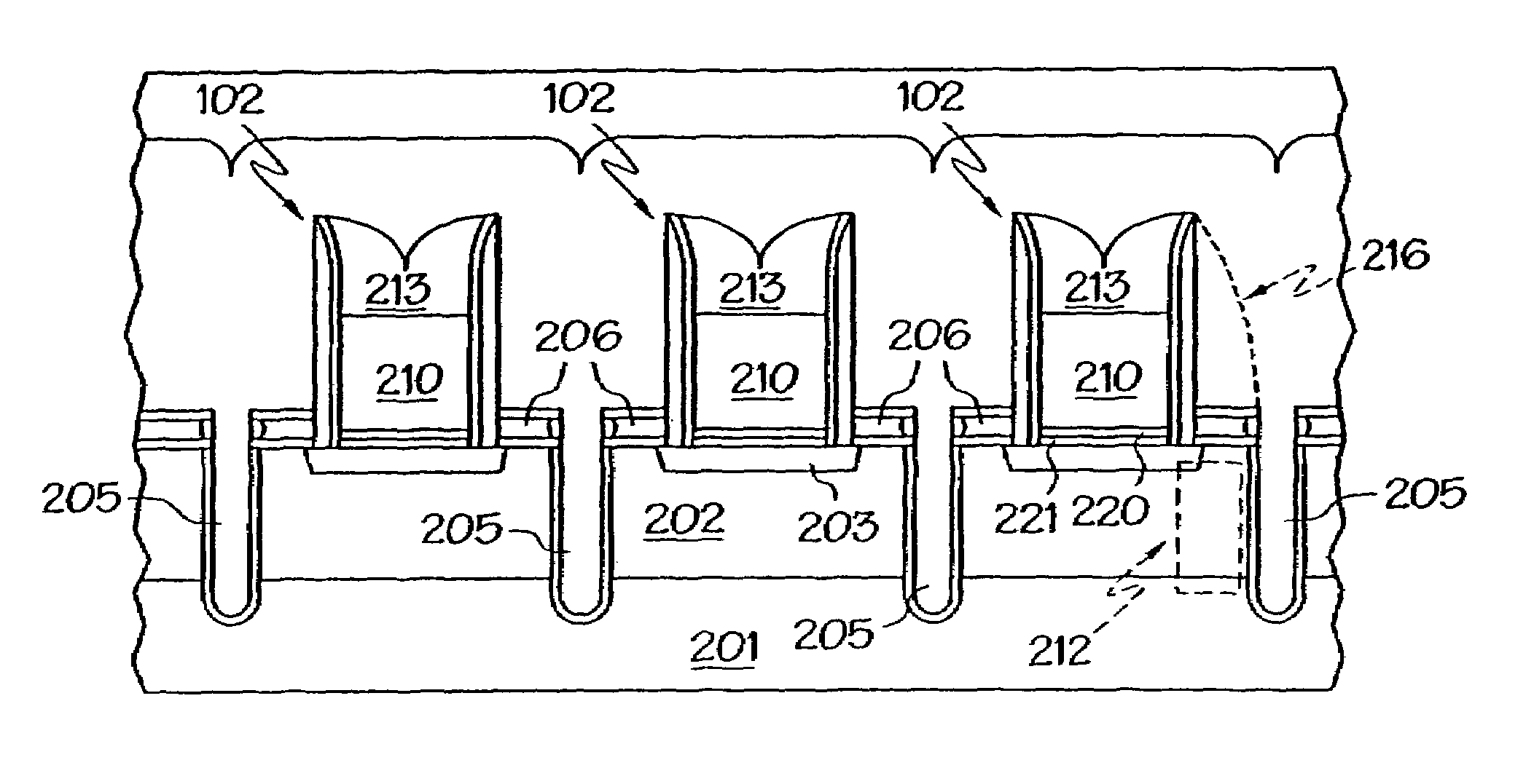
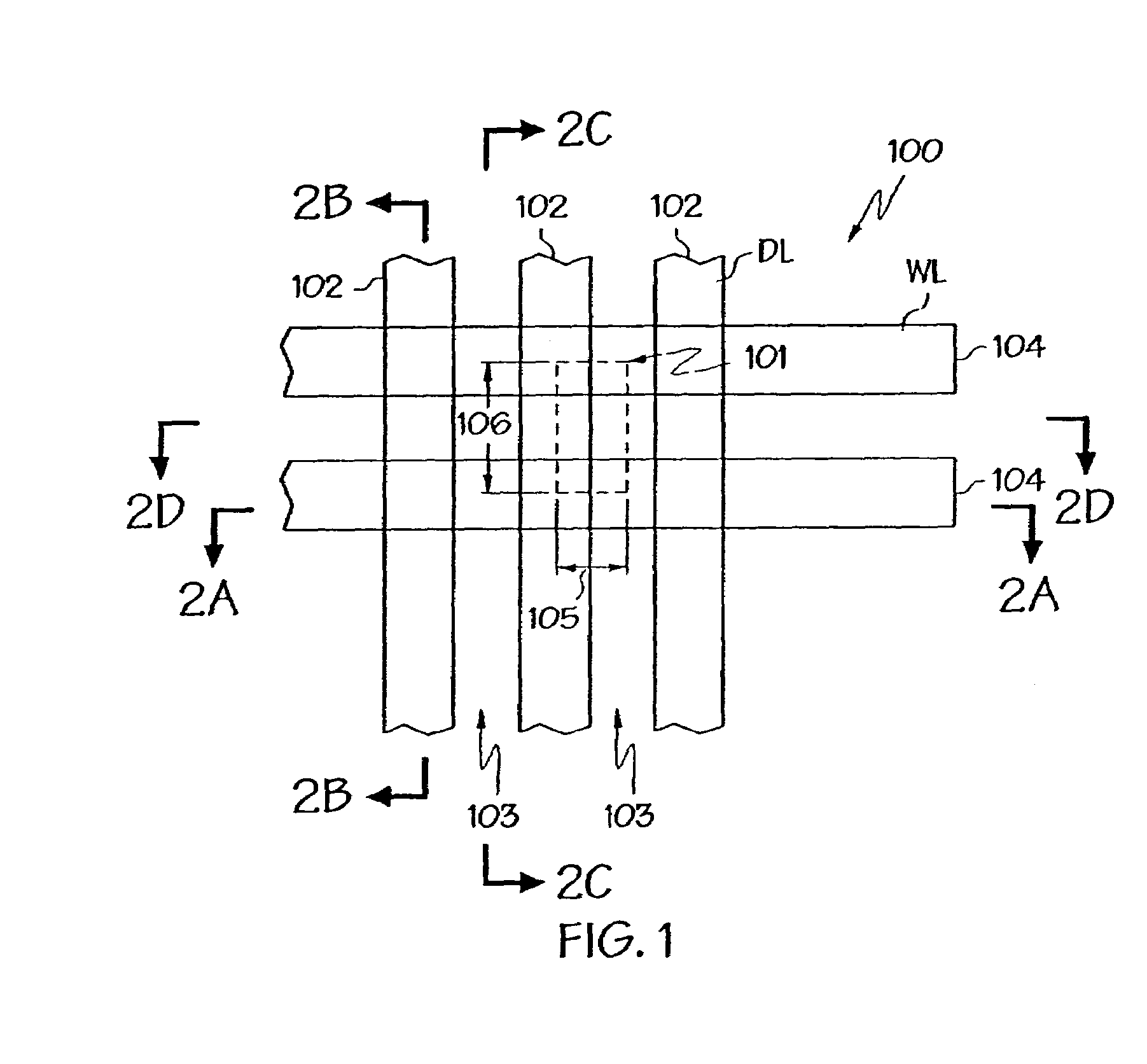
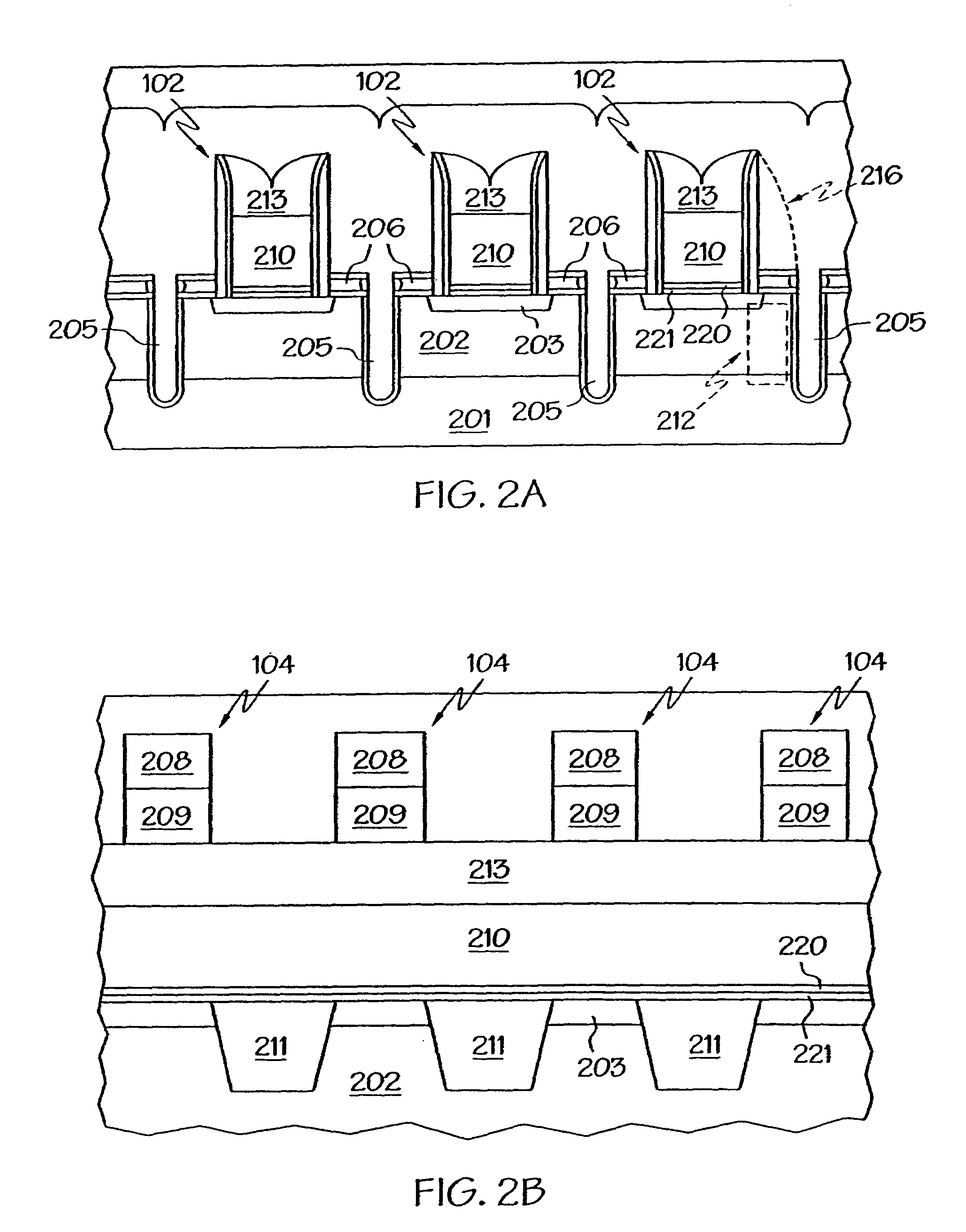
[0045]FIG. 1 illustrates a top view layout of a memory device 100 according to one embodiment of the present invention. This memory device 100 is generally used for flash memory, but can be used for other types of memory as well. This view illustrates wordlines 104, digitlines 102 and a unit cell or memory cell 101. The unit cell or memory cell 101 is one of many cells of the memory device 100. The memory cell has a minimum feature size of 1F or F 105 in a first dimension which is half of the digitline pitch and a feature size of 2F 106 in a second dimension which is the wordline pitch. The square feature size or feature area of the cell is thus equal to 2F2. The memory cells of this memory device 100 are formed using conventional silicon processing technology. As is described in further detail herein with reference to FIGS. 2A, 2B, 2C and 2D, a select transistor having a select gate 205, source 201 and drain 203 is formed as a part of the memory cell 101. The select gate 205 and a ...


PUM


Abstract

Methods and devices are disclosed which provide for memory devices having reduced memory cell square feature sizes. Such square feature sizes can permit large memory devices, on the order of a gigabyte or large, to be fabricated on one chip or die. The methods and devices disclosed, along with variations of them, utilize three dimensions as opposed to other memory devices which are fabricated in only two dimensions. Thus, the methods and devices disclosed, along with variations, contains substantially horizontal and vertical components.

Description

CROSS-REFERENCE TO RELATED APPLICATIONS[0001]This application is a division of U.S. patent application Ser. No. 09 / 802,234, filed Mar. 8, 2001, now U.S. Pat. No. 6,759,707.BACKGROUND OF THE INVENTION[0002]The present invention relates to the field of semiconductor manufacture and, more particularly, to a 2F2 flash memory.[0003]As computers become increasingly complex, the need for improved memory storage increases. At the same time, there is a continuing drive to reduce the size of computers and memory devices. Accordingly, a goal of memory device fabrication is to increase the number of memory cells per unit area.[0004]Memory devices contain blocks or arrays of memory cells. A memory cell stores one bit of information. Bits are commonly represented by the binary digits 0 and 1. A flash memory device is a non-volatile semiconductor memory device in which contents in a single cell or a block of memory cells are electrically programmable and may be read or written in a single operatio...

Claims


Application Information

Patent Timeline
IPC IPC(8): H01L21/336H01L21/8247H01L27/115H01L29/788H01L29/792
CPCH01L27/115H01L29/7883H01L27/11556H10B69/00H10B41/27
Inventor PRALL, KIRK
Owner MICRON TECH INC
Why Eureka
Try Eureka