Thermal processing apparatus and thermal processing method

a technology of thermal processing apparatus and thermal processing method, which is applied in the direction of drying solid materials, drying machines, baking ovens, etc., can solve the problems of heterogeneous thermal processing of substrates, short flashing time, and the need to implant ions disadvantageously beyond necessity, so as to achieve the effect of ensuring the intensity of irradiation

Inactive Publication Date: 2006-02-14
DAINIPPON SCREEN MTG CO LTD
View PDF15 Cites 62 Cited by
  • Summary
  • Abstract
  • Description
  • Claims
  • Application Information

AI Technical Summary

Benefits of technology

[0013]The thermal processing apparatus can control the intensity of irradiation by adjusting the distance of irradiation while keeping a discharge voltage applied to the flash lamps constant. Thus, the thermal processing apparatus using flash lamps can readily control the intensity of irradiation.
[0015]The distance between the surface of the substrate and the plurality of flash heating elements is set to at least 40 mm and not more than 100 mm, so that the thermal processing apparatus can homogeneously thermally process the substrate also when using the plurality of flash heating elements.
[0017]Accordingly, an object of the present invention is to provide a thermal processing apparatus capable of readily controlling the intensity of irradiation also when employing a flash lamp.

Problems solved by technology

In this case, the ions are diffused even if the same are implanted into the surface of the semiconductor wafer in high concentration, and hence the ions must be implanted disadvantageously beyond necessity.
When such a thermal processing apparatus is provided with a plurality of xenon flash lamps, however, a heat gradient corresponding to the light intensity gradient of the xenon flash lamps takes place on the substrate, to disadvantageously result in heterogeneous thermal processing of the substrate.
In the thermal processing apparatus employing the flash lamps, however, the time for emitting flashes is so short that the problem of the heat gradient cannot be solved by rotating the substrate.
In the case of the thermal processing apparatus employing xenon flash lamps, however, a method of adjusting the intensity of irradiation by changing a main discharge voltage applied to the lamps results in various demerits.
In other words, not only the intensity of irradiation but also optical characteristics of the flashes vary when the main discharge voltage applied to the lamps is simply changed, to result in disintegration of correlation between the intensity of irradiation and the wafer temperature, leading to extreme difficulty of temperature control.
When the main discharge voltage applied to the xenon flash lamps is changed, degradation characteristics of the lamps are also disadvantageously varied.

Method used


Image

  • Thermal processing apparatus and thermal processing method
  • Thermal processing apparatus and thermal processing method
  • Thermal processing apparatus and thermal processing method

Examples


first embodiment

[0026]

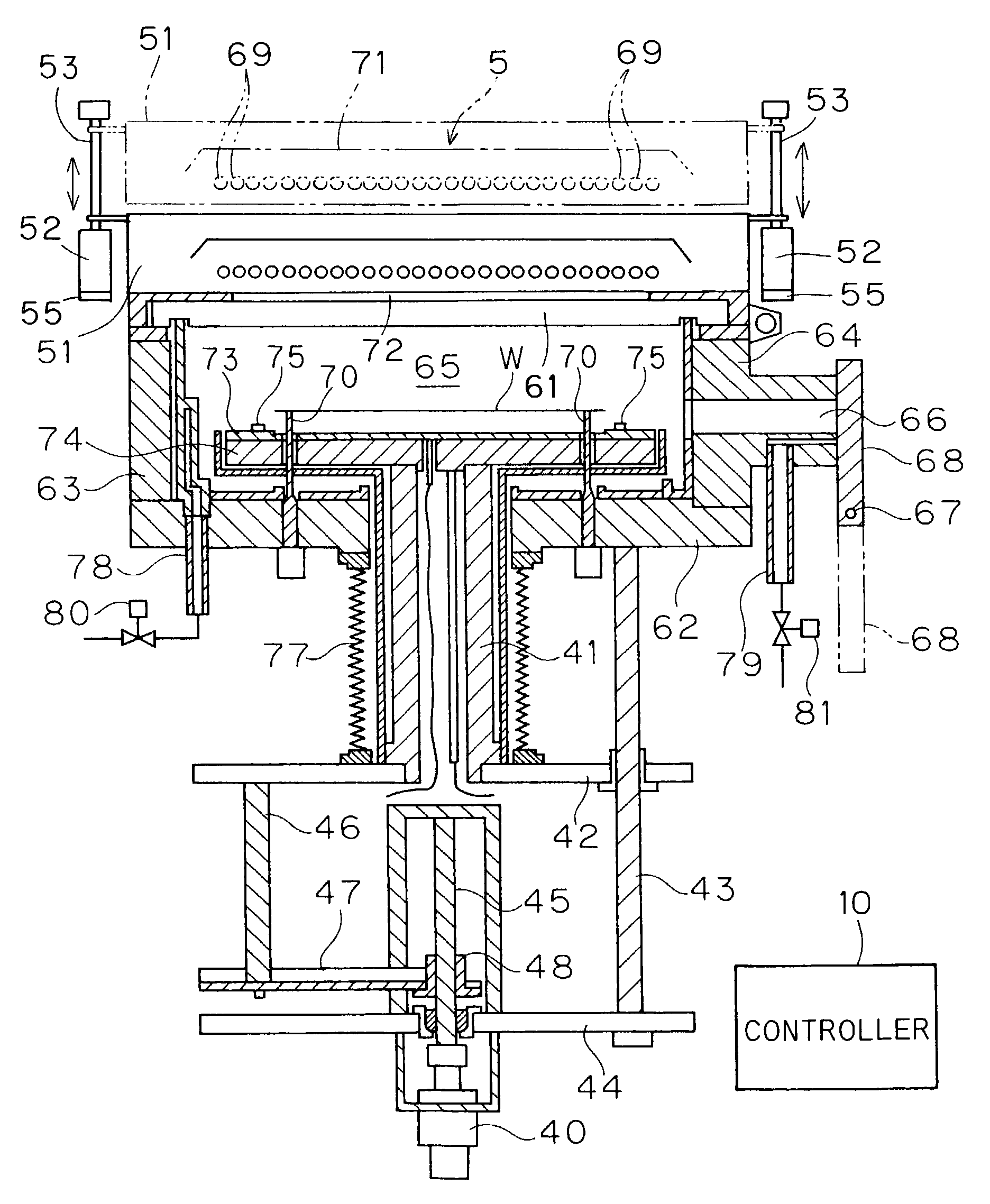
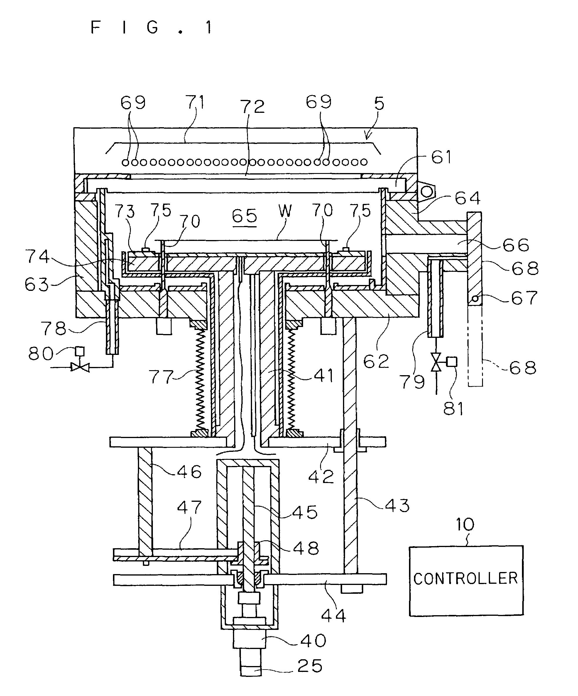
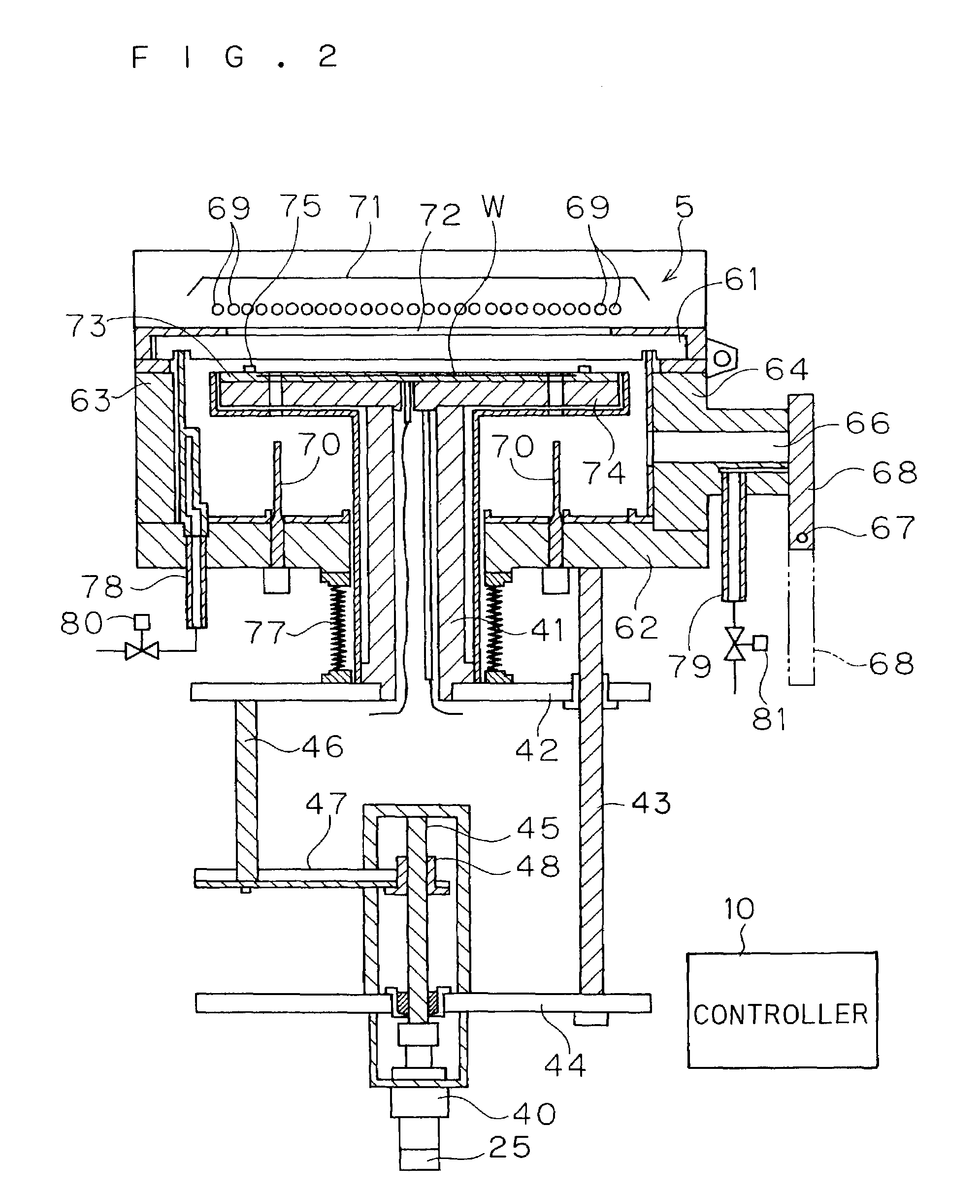
[0027]FIGS. 1 and 2 are cross-sectional views showing a thermal processing apparatus according to a first embodiment of the present invention. This thermal processing apparatus thermally processes substrates such as semiconductor wafers with flashes emitted from xenon flash lamps.

[0028]This thermal processing apparatus comprises a chamber 65 consisting of a translucent plate 61, a base plate 62 and a pair of side plates 63 and 64 for storing and thermally processing a semiconductor wafer W therein. The translucent plate 61 forming the upper portion of the chamber 65 is made of an infrared-transparent material such as quartz, for example, for serving as a chamber window transmitting light emitted from a light source 5 and guiding the same into the chamber 65. Support pins 70 are uprightly provided on the base plate 62 forming the chamber 65 for supporting the semiconductor wafer W from under the lower surface thereof through a thermal diffuser 73 and a hot plate 74 described la...

second embodiment

[0063]

[0064]A thermal processing apparatus according to a second embodiment of the present invention is now described. While the thermal processing apparatus according to the aforementioned first embodiment adjusts the distance of irradiation by adjusting the positions of the thermal diffuser 73 and the hot plate 74 holding the semiconductor wafer W, the thermal processing apparatus according to the second embodiment adjusts the distance of irradiation by adjusting the position of a light source 5. FIG. 5 is a cross-sectional view showing the thermal processing apparatus according to the second embodiment of the present invention. Members similar to those of the thermal processing apparatus according to the aforementioned first embodiment are denoted by the same reference numerals, to omit redundant description.

[0065]In the thermal processing apparatus according to the second embodiment, a ball screw 53 rotated by a pair of motors 52 vertically moves a casing 51 storing flash lamps ...

third embodiment

[0069]

[0070]A thermal processing apparatus according to a third embodiment of the present invention is now described. The structure of the thermal processing apparatus according to the third embodiment is identical to that according to the first embodiment, and hence redundant description is omitted. When a semiconductor wafer W is arranged on a thermal processing position in the thermal processing apparatus according to the third embodiment, the distance between the surface of the semiconductor wafer W and each xenon flash lamp 69 is at least 40 mm and not more than 100 mm. The distance between the surface of the semiconductor wafer W and each xenon flash lamp 69 can be set to an arbitrary value in the range of at least 40 mm and not more than 100 mm by controlling the rotational frequency of a motor 40.

[0071]The thermal processing apparatus according to the third embodiment also thermally processes the semiconductor wafer W similarly to the first embodiment. In a flash heating ste...


PUM

PropertyMeasurementUnit
temperatureaaaaaaaaaa
distanceaaaaaaaaaa
distanceaaaaaaaaaa

Abstract

A light source comprising a plurality of flash lamps emits flashes thereby flash-heating a semiconductor wafer held by a thermal diffuser and a hot plate. The current distance of irradiation between the thermal diffuser and the hot plate holding the semiconductor wafer and the light source is so adjusted as to attain predetermined intensity of irradiation. The distance of irradiation between the thermal diffuser and the hot plate and the light source can be changed or corrected by vertically moving the thermal diffuser and the hot plate. Thus provided is a thermal processing apparatus using the flash lamps, capable of readily controlling the intensity of irradiation.

Description

BACKGROUND OF THE INVENTION[0001]1. Field of the Invention[0002]The present invention relates to a thermal processing apparatus and a thermal processing method of irradiating a semiconductor wafer or a glass substrate (hereinafter simply referred to as “substrate”) with a flash thereby thermally processing the substrate.[0003]2. Description of the Background Art[0004]In general, a thermal processing apparatus such as a lamp annealing apparatus employing a halogen lamp is used in an ion activation step for a semiconductor wafer subsequent to an ion implantation step. This thermal processing apparatus heats (anneals) the semiconductor wafer to a temperature of about 1000° C. to 1100° C., for example, thereby executing ion activation of the semiconductor wafer. The thermal processing apparatus increases the temperature of the substrate at a speed of about several 100 degrees per second through the energy of light emitted from the halogen lamp.[0005]However, it has been proved that the ...

Claims


Application Information

Patent Timeline
Patent Type & Authority Patents(United States)
IPC IPC(8): F27D11/00H01L21/00
CPCF27B17/0025F27D5/0037H01L21/67248F27D99/0006H01L21/67115F27D19/00
Inventor KUSUDA, TATSUFUMIIMAOKA, YASUHIROMURAYAMA, HIROMIYAMAMOTO, NORIOMORI, NAOTOYOSHIHARA, YOKO
Owner DAINIPPON SCREEN MTG CO LTD
Why Eureka
Try Eureka