
Organic EL panel drive circuit and organic EL display device using the same drive circuit

a drive circuit and drive circuit technology, applied in static indicating devices, instruments, electroluminescent light sources, etc., can solve the problems of insufficient restriction of luminous variation on the display screen of the organic el display panel, luminous variation variation of the luminous intensity etc., to achieve reduced output current, high pairing characteristics, and reduced luminous variation of the organic el elements corresponding to the terminal pins

Active Publication Date: 2006-02-21
ROHM CO LTD
View PDF9 Cites 0 Cited by
  • Summary
  • Abstract
  • Description
  • Claims
  • Application Information

AI Technical Summary

Benefits of technology

[0029]An object of the present invention is to provide an organic EL drive circuit, which can reduce luminous variation on an organic EL display panel.
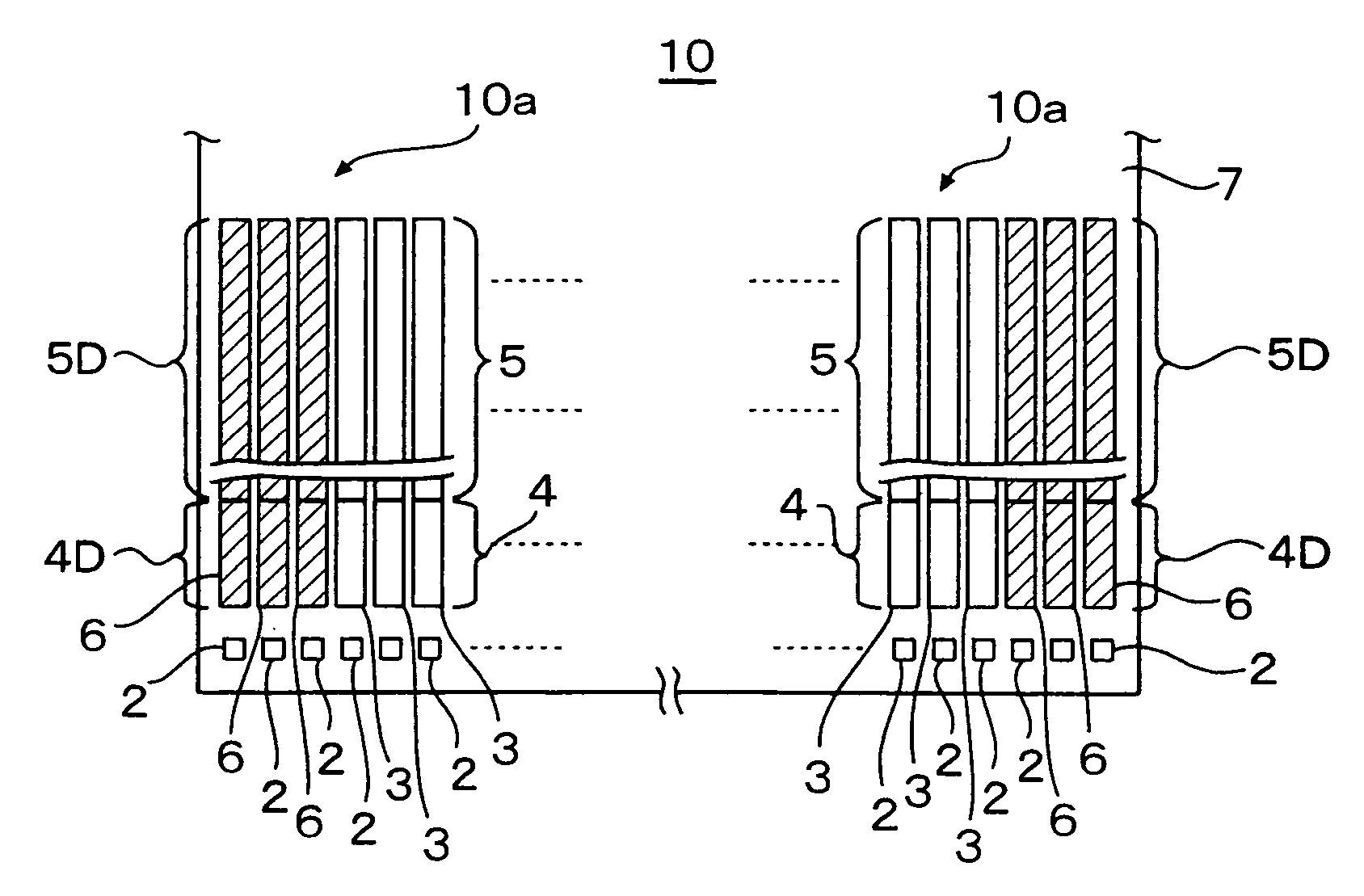
[0033]In the present invention, since the transistor blocks provided in opposite ends of the drive circuit forming area of the IC chip are the dummy circuits, the difference in physical property between the transistors, which are formed in the transistor blocks inside the transistor block forming area and forming the D / A converters or the D / A converters and the current sources, is reduced, so that the current mirror circuits of the D / A converters can be constructed with transistors having high pairing characteristics.
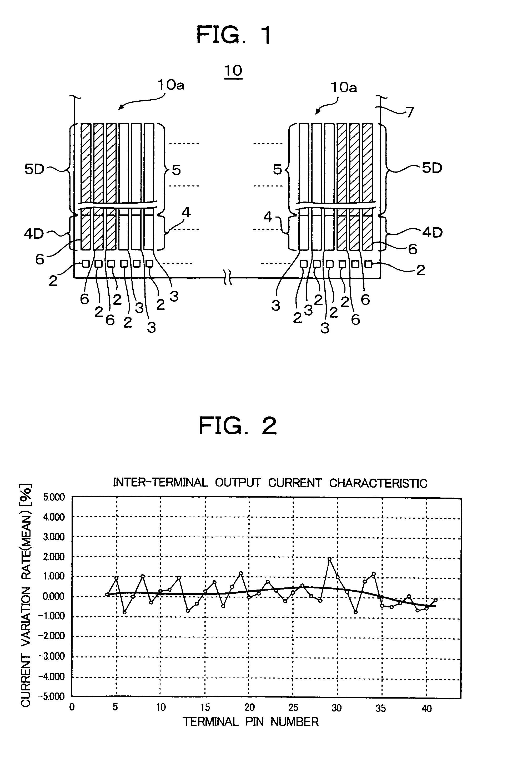
[0034]Therefore, the reduction of output currents to be supplied to the outermost terminal pins is restricted and the luminous variation of the organic EL elements corresponding to the terminal pins can be reduced. As such, the influence of the luminous variation on a luminous variation of every organic EL display device can be reduced.

Problems solved by technology

In a case where large drive currents in the order of milli-ampere or ampere are generated on the basis of a reference current in the order of several micro amperes by the organic EL element drive circuit in which the drive currents are generated by using the D / A converter circuit having the current mirror circuit construction mentioned previously, there is a problem that variation of conversion accuracy of the D / A converter circuit causes variation of output current of an output stage current source, resulting in a luminous variation.
As a result, the difference in output current between terminal pins corresponding to the current mirror circuits becomes large, resulting in variation of luminous intensity of the organic EL elements.
Even if the reference current is distributed by arranging the input side transistor of the current mirror circuit in the center portion of the output side transistors as disclosed in U.S. Pat. No. 6,586,888, it is impossible to sufficiently restrict the luminous variation on the display screen of the organic EL display panel.

Method used


Image

  • Organic EL panel drive circuit and organic EL display device using the same drive circuit
  • Organic EL panel drive circuit and organic EL display device using the same drive circuit
  • Organic EL panel drive circuit and organic EL display device using the same drive circuit

Examples


Embodiment Construction

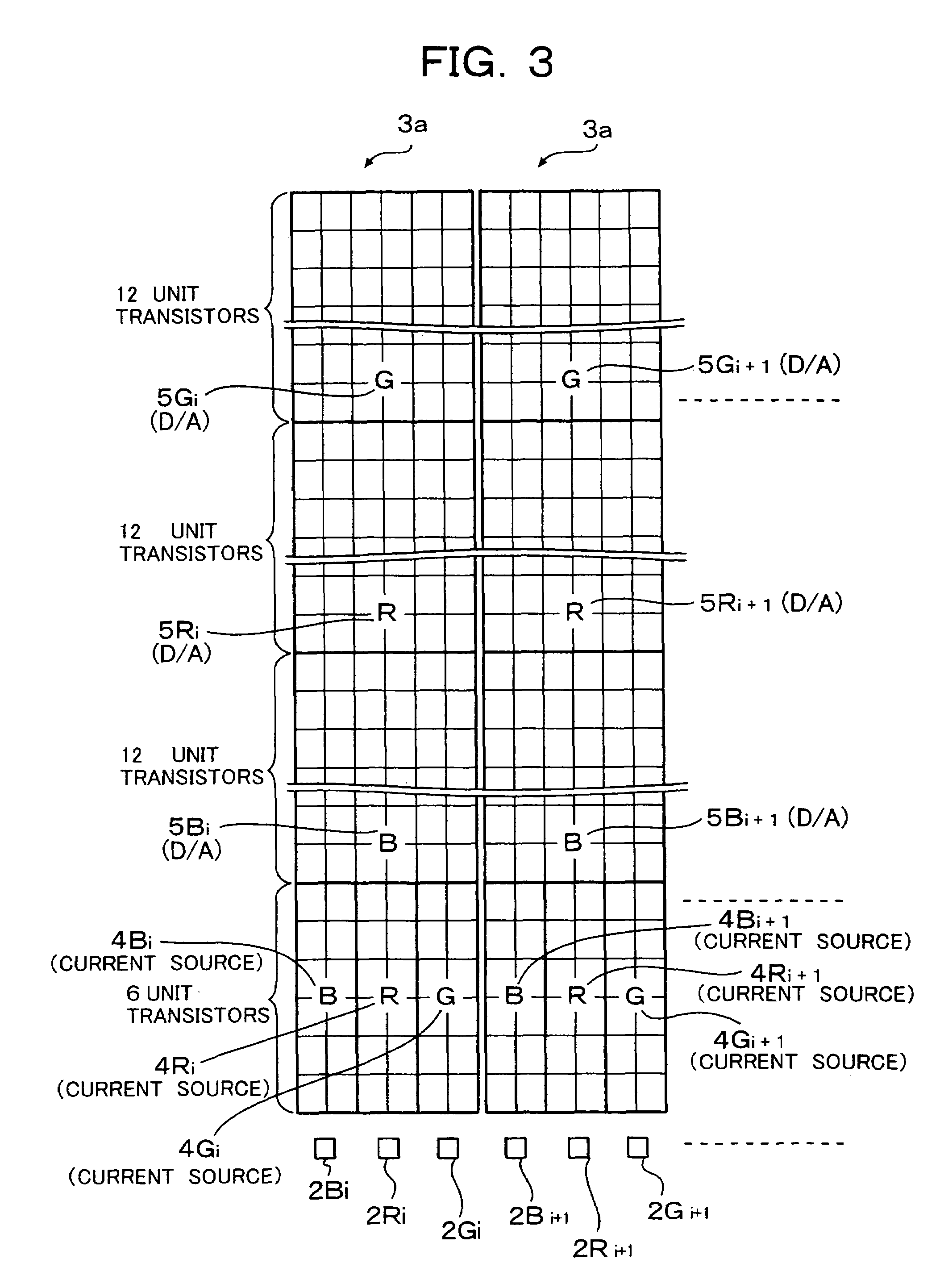
[0042]Constructive components shown in FIG. 1 and FIG. 3, which are the same as those shown in FIG. 4(a) to FIG. 4(c), are depicted by same reference numerals, respectively.

[0043]FIG. 1 shows a layout of unit transistor blocks formed in a transistor block forming area 7 of a column driver IC 10 of an organic EL drive circuit, according to an embodiment of the present invention. In FIG. 1, a reference numeral 10a depicts a layout of the unit transistor blocks each including unit transistors constituting a D / A converter circuit and an output stage current source, which are provided correspondingly to terminal pins of an organic EL display panel.

[0044]A transistor block 3 includes two columns each including 42 unit transistors similarly to the transistor block 3 shown in FIG. 4(a). Hatched transistor blocks 6 each similar to the transistor block 3 are dummy blocks forming dummy circuits, which are not used to drive organic EL elements arranged in a matrix.

[0045]A set of three transisto...


PUM


Abstract

Dummy circuits, which are not operated, are provided in transistor blocks, which are positioned in outermost side portions of a drive circuit forming area of an IC. Physical property-related stress of unit transistors constituting D / A converter circuits or the D / A converter circuits and output stage current sources, which are formed in the transistor block in an area between the outermost transistor blocks, are relatively even, so that current mirror circuits constituting the D / A converter circuits can be constructed with unit transistors having good pairing characteristics.

Description

BACKGROUND OF THE INVENTION[0001]1. Field of the Invention[0002]The present invention relates to an EL (electro luminescent) element drive circuit and an organic EL display device using the same drive circuit. In particular, the present invention relates to a circuit layout of a current drive circuit for driving organic EL elements having anodes connected to a column line of an organic EL panel of an organic EL display device through terminal pins of the organic EL panel by currents generated by a D / A converter circuit constituted with a current mirror circuit, with which luminous variation of the organic EL elements can be reduced to reduce influence thereof on luminous variation of every organic EL display device.[0003]2. Description of the Prior Art[0004]An organic EL display panel of an organic EL display device, which is mounted on a portable telephone set, a PHS, a DVD player or a PDA (personal digital assistance) and includes 396 (132×3) terminal pins for column lines and 162...

Claims


Application Information

Patent Timeline
IPC IPC(8): G09G3/10G09G3/30G09G3/32H05B33/00H05B44/00
CPCG09G3/3283G09G2310/027H01L27/3281H01L27/3223H01L27/3244G09G2320/0233H10K59/88H10K59/12H10K59/17G09G3/30H05B33/00
Inventor MAEDE, JUNABE, SHINICHIFUJIKAWA, AKIOFUJISAWA, MASANORI
Owner ROHM CO LTD
Learn More