Monolithic semiconductor device capable of suppressing mismatches between repetitive cells

a semiconductor device and repetitive cell technology, applied in the field of monolithic semiconductor devices, can solve the problems of deteriorating the differential and integral linearity of the above-mentioned a/d converter, and achieve the effect of suppressing the mismatch between repetitive cells and reducing the effect of cell mismatches

Active Publication Date: 2006-02-28
RENESAS ELECTRONICS CORP
View PDF5 Cites 0 Cited by
  • Summary
  • Abstract
  • Description
  • Claims
  • Application Information

AI Technical Summary

Benefits of technology

[0008]It is an object of the present invention to provide a monolithic semiconductor device capable of suppressing mismatches between repetitive cells, particularly, between their current sources.
[0009]According to the present invention, a monolithic semiconductor device is constructed by a plurality of repetitive cells. Each of the repetitive cells includes one circuit section and one current source for supplying a current to the circuit section. Also, a plurality of impedance circuits are connected between the current sources of two of the repetitive cells, to reduce the effect of cell mismatches among the repetitive cells.

Problems solved by technology

In the above-described prior art, however, although the mismatches resulting from deviations from nominal occurring between the differential pairs of the comparators can be suppressed, the mismatches resulting from deviations from nominal occurring between the current sources of the comparators cannot be suppressed, which still would deteriorate the differential and integral linearity of the above-mentioned A / D converter.

Method used


Image

  • Monolithic semiconductor device capable of suppressing mismatches between repetitive cells
  • Monolithic semiconductor device capable of suppressing mismatches between repetitive cells
  • Monolithic semiconductor device capable of suppressing mismatches between repetitive cells

Examples


first embodiment

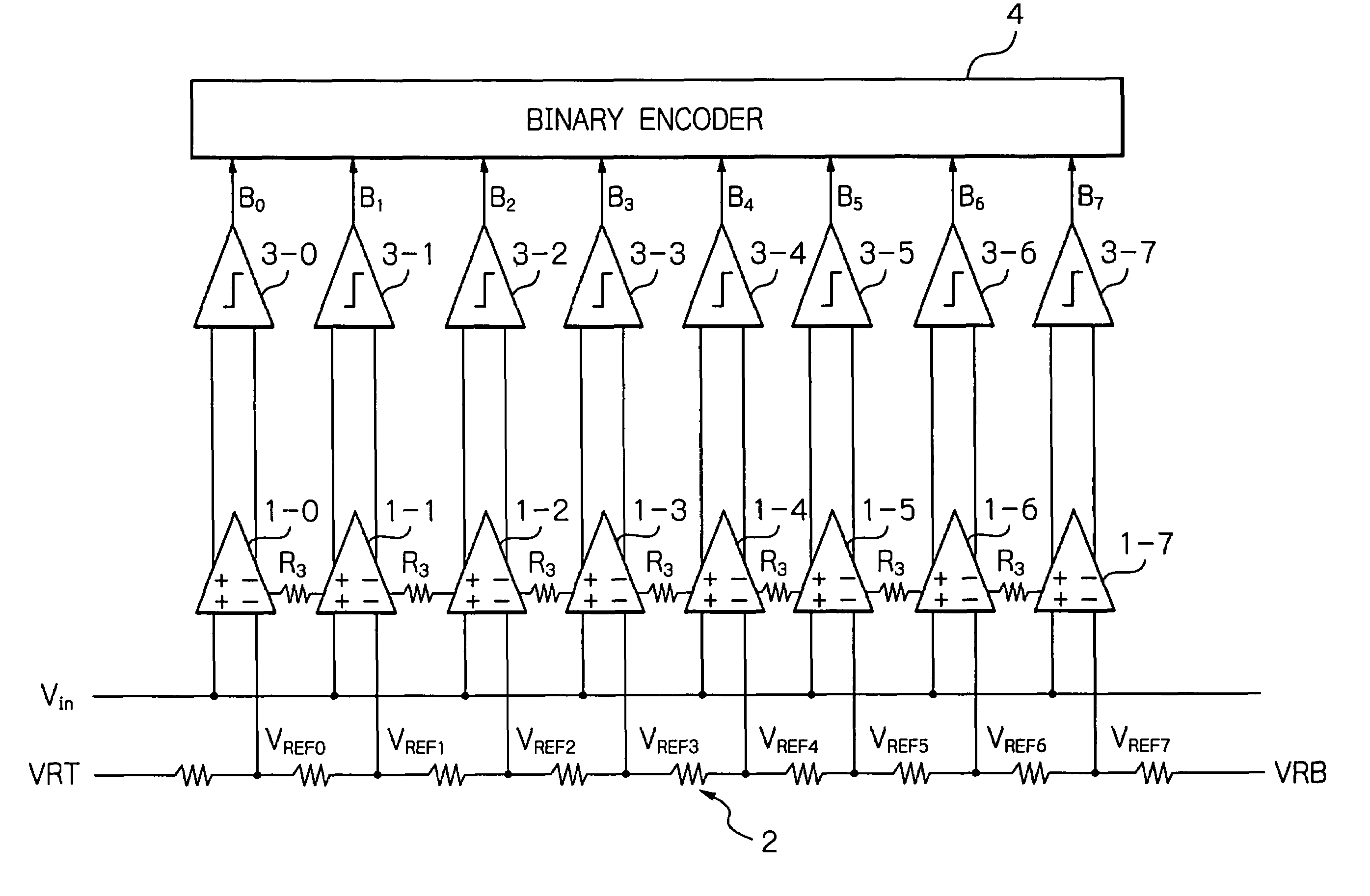
[0031]In FIG. 7, which illustrates a 3-bit flash or parallel-type A / D converter to which the monolithic semiconductor device according to the present invention is applied, resistors R3 as impedance circuits are connected between the comparators 1-0, 1-1, . . . , 1-7 of FIG. 1. In this case, it is preferable that the resistors R3 have the same value. In more detail, as shown in FIG. 8, the resistors R3 are connected between nodes N0, N1, . . . , N7 of the differential pairs 100, 101, . . . , 107 and the constant current sources 200, 201, . . . , 207.

[0032]The operation of the monolithic semiconductor device of FIG. 8 is explained next with reference to FIGS. 9, 10 and 11 where there are a large number of comparators (cells) that are indefinite in extent.

[0033]In FIG. 9, assume that a current flowing through the constant current source of a specified comparator (i=0) is deviated from nominal and can be defined as I+δI where δI is an error current. V(−4), V(−3), V(−2), V(−1), V(0), V(1...

second embodiment

[0043]In FIG. 12, which illustrates a 3-bit flash or parallel-type A / D converter to which the monolithic semiconductor device according to the present invention is applied, the resistors R2 of FIG. 4 as impedance circuits are added to the elements of FIG. 7. In more detail, as shown in FIG. 13, the resistors R2 are connected between the outputs OUTP of the differential pairs 100, 101, . . . , 107 and between the outputs OUTN of the differential pairs 100, 101, . . . , 107.

[0044]In FIGS. 12 and 13, differences in output voltage or output dynamic response between the cells are suppressed by the resistors R3, and also, the mismatches resulting from deviation from nominal occurring between the cells are suppressed by the resistors R2. Thus, the differential and integral linearity of the A / D converter would be further improved.

[0045]In the above-described embodiments, the differential pairs can be formed by bipolar transistors. Also, the present invention can be applied to other repetiti...


PUM


Abstract

A monolithic semiconductor device is constructed by a plurality of repetitive cells each including one circuit section and one current source for supplying a current to said circuit section, and a plurality of first impedance circuits, each connected between the current sources of two of the repetitive cells, for reducing the effect of cell mismatches among the repetitive cells.

Description

BACKGROUND OF THE INVENTION[0001]1. Field of the Invention[0002]The present invention relates to a monolithic semiconductor device (chip) including repetitive cells.[0003]2. Description of the Related Art[0004]For example, a flash or parallel-type analog / digital (A / D) converter is constructed by a large number of repetitive cells. That is, such an A / D converter is constructed by comparators for comparing an analog input voltage with reference voltages, latch circuits for latching the output signals of the comparators, and a binary encoder for encoding the output signals of the latch circuits. In this case, the comparators form repetitive cells in a monolithic semiconductor device. Each of the comparators is constructed by one differential pair and one current source for supplying a current thereto. This will be explained later in detail.[0005]In the above-mentioned A / D converter, when mismatches resulting from deviations from nominal occur between the repetitive cells, the different...

Claims


Application Information

Patent Timeline
Patent Type & Authority Patents(United States)
IPC IPC(8): H03M1/36H03M1/06
CPCH03M1/0646H03M1/36
Inventor NAKAJIMA, YUJI
Owner RENESAS ELECTRONICS CORP
Why Eureka
Try Eureka