Unlock instant, AI-driven research and patent intelligence for your innovation.

Diagnosable scan chain

a scan chain and scan technology, applied in the computer field, can solve the problems of significant expense incurred during the manufacture of integrated circuits, multiple offsetting errors, and defective scan chains themselves, and achieve the effect of convenient locating

Active Publication Date: 2006-02-28
TWITTER INC
View PDF10 Cites 14 Cited by
  • Summary
  • Abstract
  • Description
  • Claims
  • Application Information

AI Technical Summary

Benefits of technology

[0010]The present invention is directed to a method and system for locating connector defects in a defective scan chain that has a parallel non-defective scan chain on a different wiring level, with both scan chains being laid out in a regular array pattern. A predetermined bit sequence is scanned into the defective scan chain. The contents of the defective scan chain are then parallel shifted into the non-defective scan chain. The contents of the non-defective scan chain is then scanned out and compared with the predetermined bit sequence. The comparison of the scanned out bits with the predetermined bit sequence facilitates locating both physically and logically where a connector defect has occurred in the defective scan chain.

Problems solved by technology

A significant expense incurred during the manufacture of integrated circuit (IC) wafers is testing.
That is, a known input data into a logic circuit may result in a desired (expected) output, but the desired output may be the result of multiple offsetting errors.
While scan chains are useful in determining whether a logic circuit is functioning properly, the scan chains themselves may also be defective.
While such defects may be from defective latches in the scan chain, if the latches are robust (designed to ensure their integrity), then defects are primarily in the wiring connecting the latches.
Such defects may be opens (a clean break in the wiring), shorts (the wiring touching another wire inadvertently), or stuck-at faults (the wiring touching either ground or voltage).
The most problematic wiring defect is a stuck-at fault, since the latch otherwise appears to be functioning properly, albeit with a constant input value.

Method used


Image

  • Diagnosable scan chain
  • Diagnosable scan chain
  • Diagnosable scan chain

Examples


Embodiment Construction

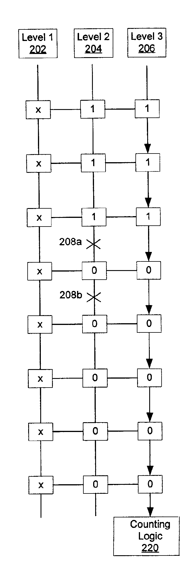
[0023]With reference now to FIG. 2a, there is illustrated an exemplary scan chain matrix 200 as used in a preferred embodiment of the present invention. Scan chain matrix 200 includes three parallel scan chains 202, 204 and 206, each in parallel with another scan chain each and having associated latches 222 corresponding between the scan chains. Scan chains 202 and 206 have no defects, but scan chain 204 has one or more defects in the connectors 250 between at least one pair of latches 222.

[0024]Latches 222 are preferably master / slave latch pairs, but may be any bit or state holding device known to those skilled in the art of integrated circuit (IC) design. In a preferred embodiment, each scan chain is physically wired on a different wiring level of an IC chip or wafer. These wiring levels are preferably on different metal levels, but may be on any different wiring level as understood by those skilled in the art of IC fabrication. Thus scan chain 202 is physically wired on wiring le...


PUM


Abstract

A method and system for locating connector defects in a defective scan chain that has a parallel non-defective scan chain on a different wiring level, with both scan chains being laid out in a regular array pattern. A predetermined bit sequence is scanned into the defective scan chain. The contents of the defective scan chain are then parallel shifted into the non-defective scan chain. The contents of the non-defective scan chain is then scanned out and compared with the predetermined bit sequence. The comparison of the scanned out bits with the predetermined bit sequence facilitates locating both physically and logically where a connector defect has occurred in the defective scan chain.

Description

BACKGROUND OF INVENTION[0001]1. Technical Field[0002]The present invention relates in general to the field of computers, and in particular to the testing of circuits, including integrated circuits. Still more particularly, the present invention relates to a method and system for locating a defect in a scan chain.[0003]2. Description of the Related Art[0004]A significant expense incurred during the manufacture of integrated circuit (IC) wafers is testing. Such testing generally entails inputting data into a logic circuit on the wafer at a first test access point, and then reading the output results at a second test access point. Often, finer granularity is required to determine whether the logic is functioning properly. That is, a known input data into a logic circuit may result in a desired (expected) output, but the desired output may be the result of multiple offsetting errors. For example, if a “1” is input into three inverters in series, a “0” will be output whether all three in...

Claims


Application Information

Patent Timeline
Patent Type & Authority Patents(United States)
IPC IPC(8): G01R31/28G06F7/02G01R31/3185
CPCG01R31/31855
Inventor EUSTIS, STEVEN MICHAELPASTEL, LEAH MARIE PFEIFERBEDNAR, THOMAS RICHARDSOPCHAK, THOMAS GREGORYOPPOLD, JEFFERY HOWARD
Owner TWITTER INC