
Socket mounted on printed circuit board

a printed circuit board and socket technology, applied in the field of sockets, can solve the problems of occupying less space, affecting the operation of the lever b>300/b>, and increasing the number of functions, so as to achieve excellent connection, excellent connection between, and excellent connection

Active Publication Date: 2006-03-07
JU TED
View PDF5 Cites 46 Cited by
  • Summary
  • Abstract
  • Description
  • Claims
  • Application Information

AI Technical Summary

Benefits of technology

[0007]The primary objective of the invention is therefore to specify a socket that guarantees an excellent connection between an IC module and a PCB and occupies less space than the conventional socket.
[0008]According to the invention, the objective is achieved by a socket mounted on a printed circuit board (PCB) in order to orientate an IC module. The socket includes an insulative housing, a plurality of contacts, at least two screw nuts and at least two screws. The insulative housing has a plurality of slots and a border projected therefrom and around the slots for orientating an electronic component. The contacts correspond to the pads and are received in the slots, respectively. The contacts further have an end exposed out of the slots and are bent. A topmost portion of the contacts is lower than a top surface of the border. The screw nuts are adjacent to the border of the insulative housing and are relative to the soldering area, so as to connect the insulative housing to the PCB via the screw nuts. The screws mate with the screw nuts and force the electronic component downward to electrically connect to the PCB. Therefore, an excellent connection between the component and the PCB is guaranteed, and the arrangement occupies a smaller space than the prior art.
[0009]To provide a further understanding of the invention, the following detailed description illustrates embodiments and examples of the invention. Examples of the more important features of the invention thus have been summarized rather broadly in order that the detailed description thereof that follows may be better understood, and in order that the contributions to the art may be appreciated. There are, of course, additional features of the invention that will be described hereinafter which will form the subject of the claims appended hereto.

Problems solved by technology

As synthetic applications for system technologies, such as multi-media, communication or computer technologies, develop, their functions grow more and more and the layout of PCBs (printed circuit boards) become more and more complex.
Furthermore, the operation of the lever 300 interferes with other components on the PCB 600.

Method used


Image

  • Socket mounted on printed circuit board
  • Socket mounted on printed circuit board
  • Socket mounted on printed circuit board

Examples


Embodiment Construction

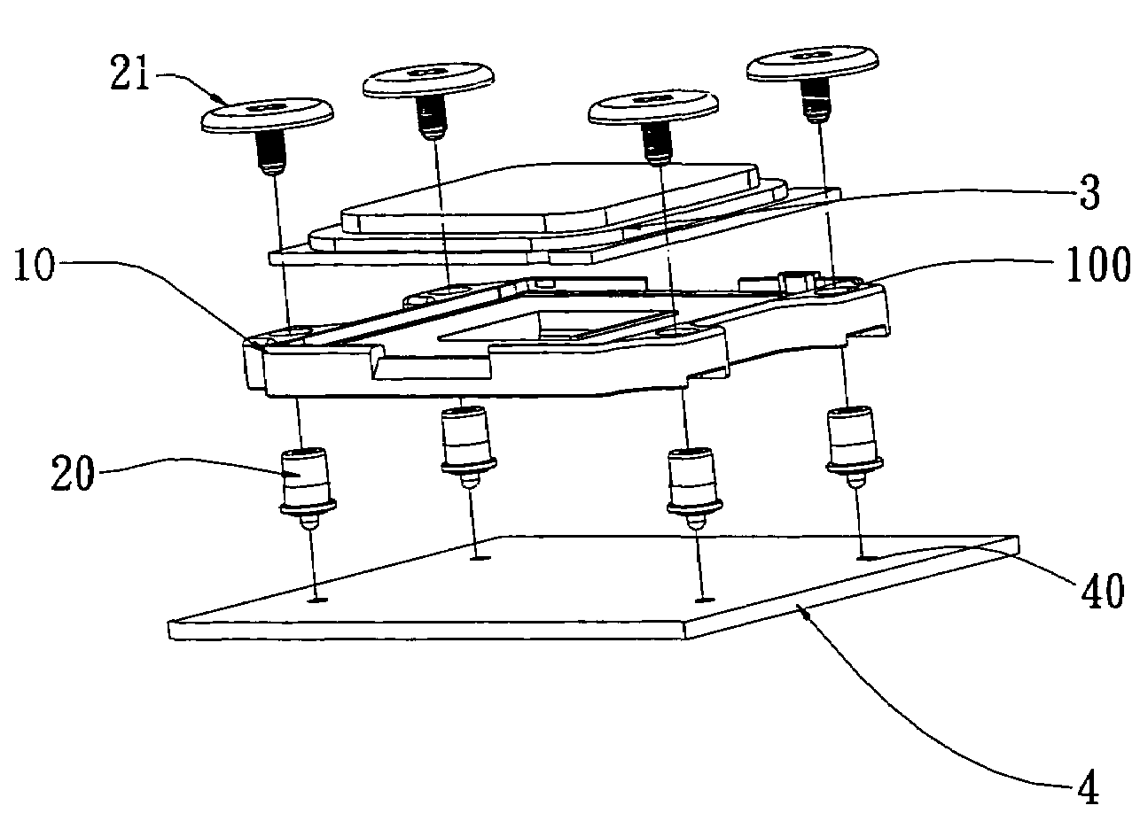
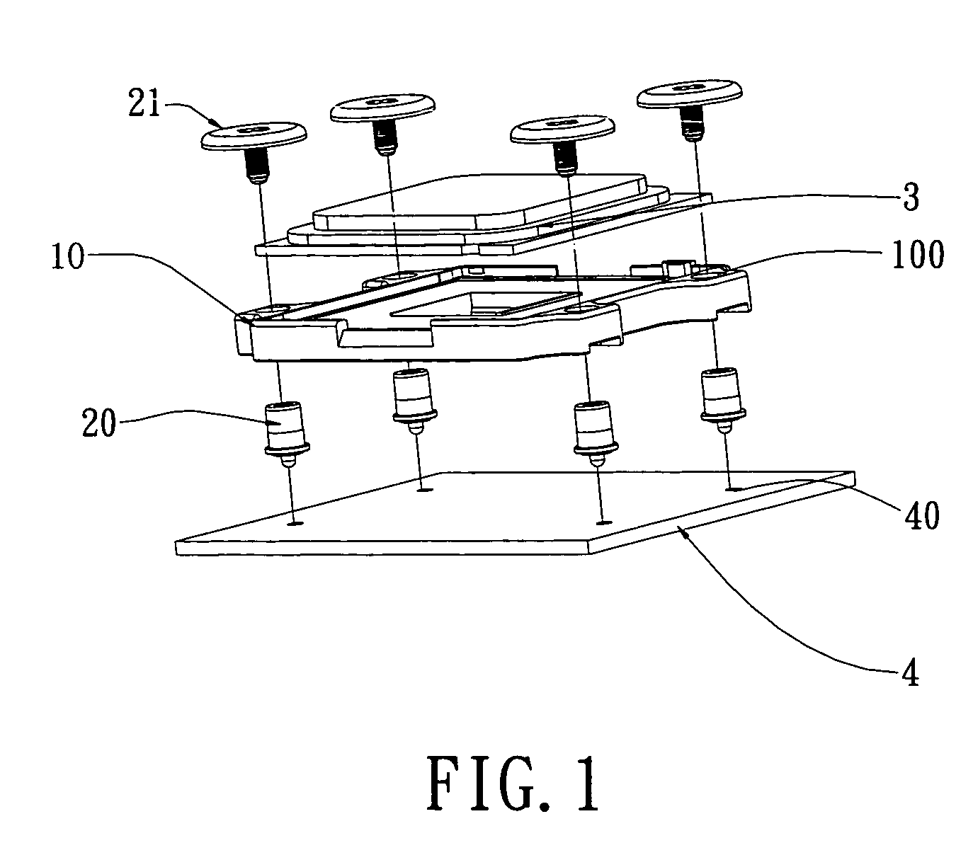
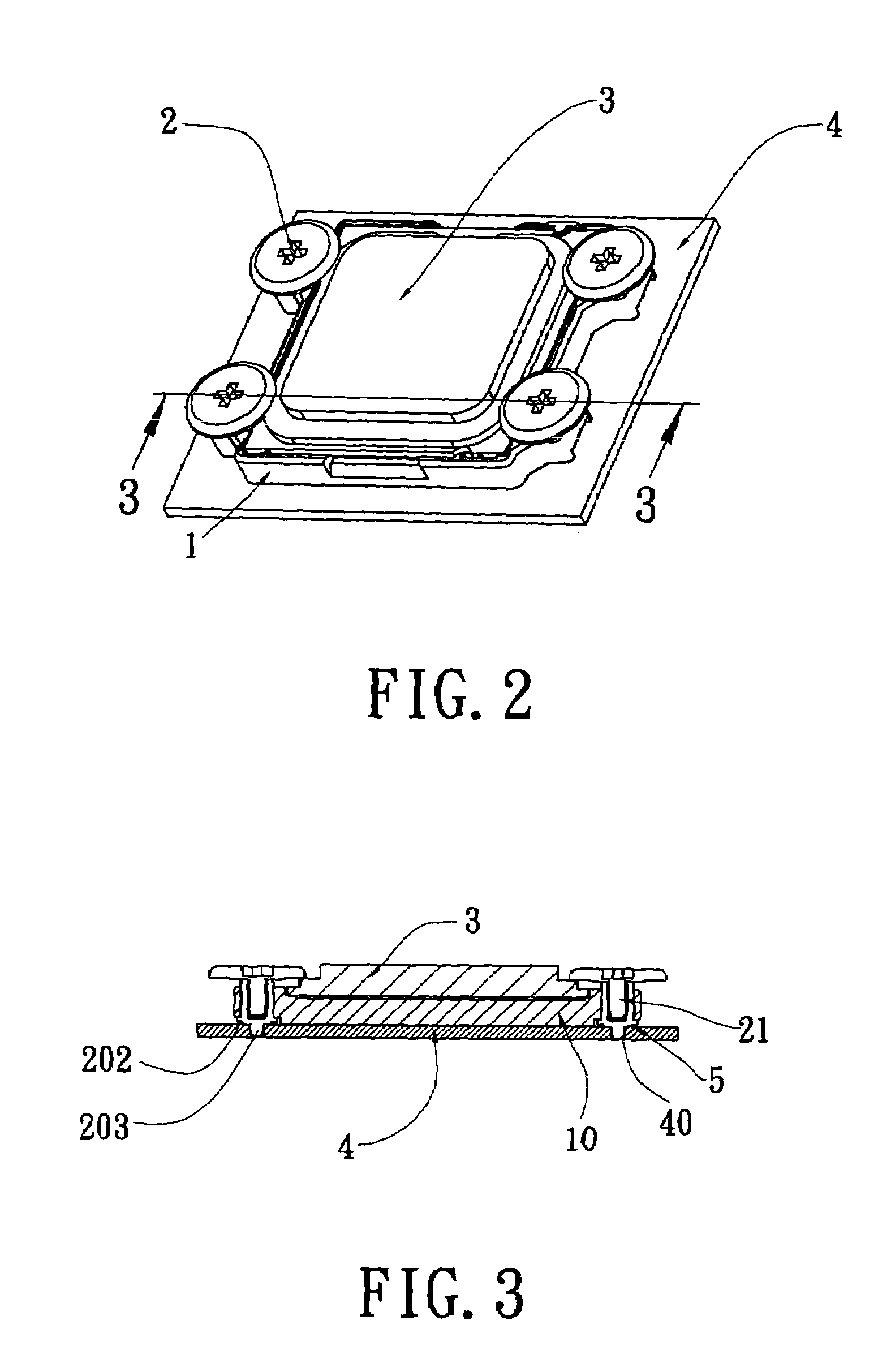
[0020]FIGS. 1 to 3 show a socket according to the present invention mounted on a printed circuit board (PCB) 4 which includes a plurality of pads and at least two soldering areas. The socket includes an insulative housing 10, a plurality of contacts, at least two screw nuts 20 and at least two screws 21. The insulative housing 10 has a plurality of slots and a border projected therefrom and around the slots for orientating an electronic component, such as an IC module 3. The contacts correspond to the pads and are received in the slots, respectively. The contacts have an end exposed out of the slots and are bent, and a topmost portion of the contacts is lower than a top surface of the border. The screw nuts 20 are adjacent to the border of the insulative housing 10 and relative to the soldering area, so as to connect the insulative housing 10 to the PCB 4 via the screw nuts 20. The screws 21 mate with the screw nuts 20 and force the electronic component 3 downward to electrically co...


PUM


Abstract

A socket mounted on a printed circuit board (PCB), which includes a plurality of pads and at least two soldering areas, includes an insulative housing, a plurality of contacts corresponding to the pads and received in the slots respectively, at least two screw nuts and at least two screws mating with the screw nuts. The insulative housing has a plurality of slots and a border projected therefrom and around the slots for orientating an electronic component. The contacts have an end exposed out of the slots and are bent, and a topmost portion of the contacts is lower than a top surface of the border. The screw nuts are adjacent to the border of the insulative housing and are relative to the soldering area, so as to connect the insulative housing to the PCB via the screw nuts. The screws force the electronic component downward to electrically connect the PCB.

Description

BACKGROUND OF THE INVENTION[0001]1. Field of the Invention[0002]The present invention relates to a socket, and particularly relates to a socket adapted for a land grind array IC module.[0003]2. Background of the Invention[0004]As synthetic applications for system technologies, such as multi-media, communication or computer technologies, develop, their functions grow more and more and the layout of PCBs (printed circuit boards) become more and more complex. Within a notebook, particularly one which has limited space for arranging all elements and components therein, the design and the layout of the PCB are extremely important.[0005]Referring to FIGS. 8 and 9, that show a conventional socket electrically connected to an IC module 500 and a PCB 600. A conventional socket includes a metallic upper hous ing 100, a metallic lower housing 200 and a lever 300, which connect to the metallic upper housing 100 and the metallic lower housing 200. In actual practice, the lever 300 occupies much ...

Claims


Application Information

Patent Timeline
Patent Type & Authority Patents(United States)
IPC IPC(8): H01R12/00
CPCH01R12/7047H01R12/714
Inventor JU, TED
Owner JU TED
Features
  • Generate Ideas
  • Intellectual Property
  • Life Sciences
  • Materials
  • Tech Scout
  • Unparalleled Data Quality
  • Higher Quality Content
  • 60% Fewer Hallucinations
Learn More