Method of manufacturing a photomask and method of manufacturing a semiconductor device using the photomask

a manufacturing method and technology applied in the field of manufacturing a photomask and a manufacturing method of a semiconductor device using a photomask, can solve the problems of dimensional accuracy required of photomasks, and reducing the yield of non-defective products

a manufacturing method and technology applied in the field of manufacturing a photomask and a manufacturing method of a semiconductor device using a photomask, can solve the problems of dimensional accuracy required of photomasks, and reducing the yield of non-defective products

US7008731B2Active Publication Date: 2006-03-07KIOXIA CORP

Image

  • Method of manufacturing a photomask and method of manufacturing a semiconductor device using the photomask
  • Method of manufacturing a photomask and method of manufacturing a semiconductor device using the photomask
  • Method of manufacturing a photomask and method of manufacturing a semiconductor device using the photomask

Examples


Embodiment Construction

[0025]An embodiment of the present invention will be described hereinafter with reference to the accompanying drawings. In the description which follows, corresponding parts are denoted by like reference characters.

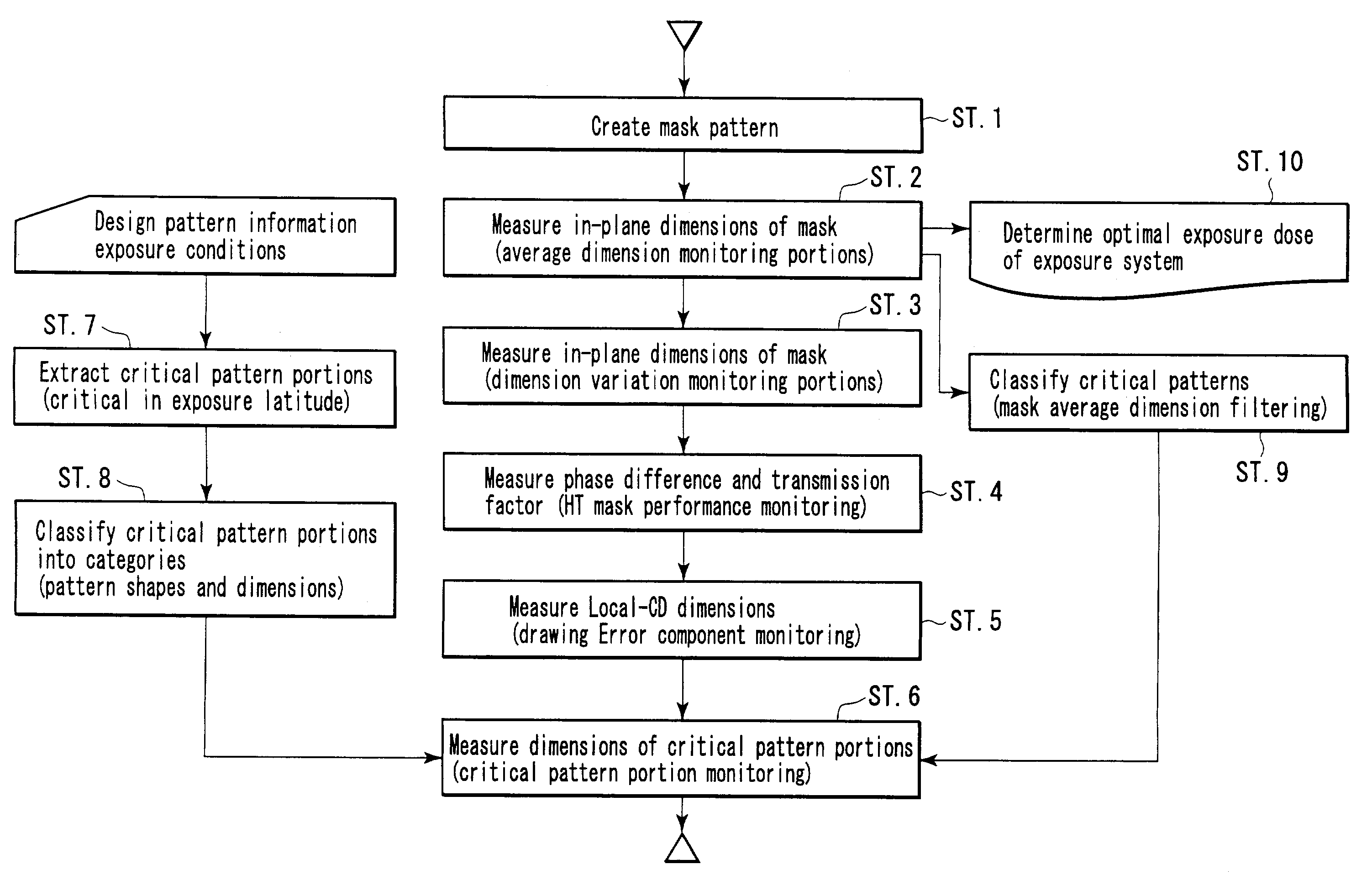
[0026]FIG. 1 is a flowchart illustrating a method of manufacturing a photomask in accordance with an embodiment of the present invention. The first embodiment is an application of the present invention to a half-tone phase-shifting mask (hereinafter referred to as an HT mask) as a photomask. It should however be noted that the present invention can be applied not only to HT masks but also to phase-shifting masks other than the HT masks and photomasks other than the phase-shifting masks, as described in U.S. patent application Ser. No. 09 / 940,578. Present application is based upon and claims the benefit of prior U.S. patent application Ser. No. 09 / 940,578, filed Aug. 29, 2001, the entire contents of which are incorporated herein by reference.

[0027]As shown in FIG. 1, mask ...


PUM

PropertyMeasurementUnit
dimensionsaaaaaaaaaa
exposure latitudeaaaaaaaaaa
shapeaaaaaaaaaa

Abstract

A method of manufacturing a photomask includes determining dimensions of a pattern in a photomask, determining an exposure latitude on the basis of the dimensions of the mask, and judging if the photomask is defective or non-defective on the basis of whether or not the exposure latitude falls within a prescribed exposure latitude. The pattern in the photomask includes dimensions of critical pattern portions in which an exposure latitude is low.

Description

CROSS-REFERENCE TO THE RELATED APPLICATIONS[0001]This application is based upon and claims the benefit of priority from the prior Japanese Patent Application No. 2002-054774, filed Feb. 28, 2002, the entire contents of which are incorporated herein by reference.BACKGROUND OF THE INVENTION[0002]1. Field of the Invention[0003]The present invention relates to a method of manufacturing a photomask and a method of manufacturing a semiconductor device using the photomask.[0004]2. Description of the Related Art[0005]The manufacturing process for semiconductor devices involves the patterning process of forming various patterns on a semiconductor wafer, the so-called lithography process. The lithography process uses photomasks.[0006]In recent years, the dimensional accuracy required of photomasks has become increasingly severe. For example, the in-plane dimensional uniformity of the photomask is required to be 10 nm or less. In the manufacture of photomasks, there is a large number of items ...

Claims


Application Information

Patent Timeline
07 Mar 2006
Publication
US7008731B2
IPC
G03F9/00; G03C5/00; G03F1/32; G03F1/36; G03F1/68; G03F7/20; H01L21/027
CPC
G03F1/84; G03F7/70625; G03F7/705; A24B15/16; A24B15/28; A24D1/18
Inventors
NOJIMA, SHIGEKI; IKENAGA, OSAMU