Active matrix type electroluminescence display device

a display device and active matrix technology, applied in static indicating devices, identification means, instruments, etc., can solve the problems of capacitance line potential , differences in luminance throughout the display device, etc., and achieve the effect of preventing voltage drops in the capacitance lin

Inactive Publication Date: 2006-03-07
SANYO ELECTRIC CO LTD
View PDF11 Cites 17 Cited by
  • Summary
  • Abstract
  • Description
  • Claims
  • Application Information

AI Technical Summary

Benefits of technology

[0014]With this structure, because a constant voltage is supplied from both ends of the capacitance lines, voltage drops in the capacitance lines can be prevented, th

Problems solved by technology

However, in larger size conventional EL display devices, differences in luminance throughout the display device have been observed.
However, when the resistance value of the capacitance line 17 is large, the potential

Method used


Image

  • Active matrix type electroluminescence display device
  • Active matrix type electroluminescence display device
  • Active matrix type electroluminescence display device

Examples


Embodiment Construction

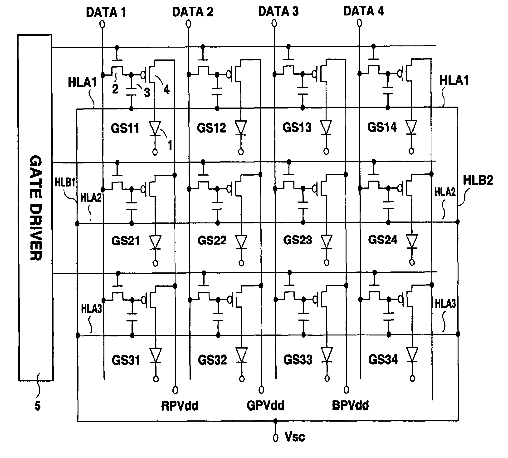
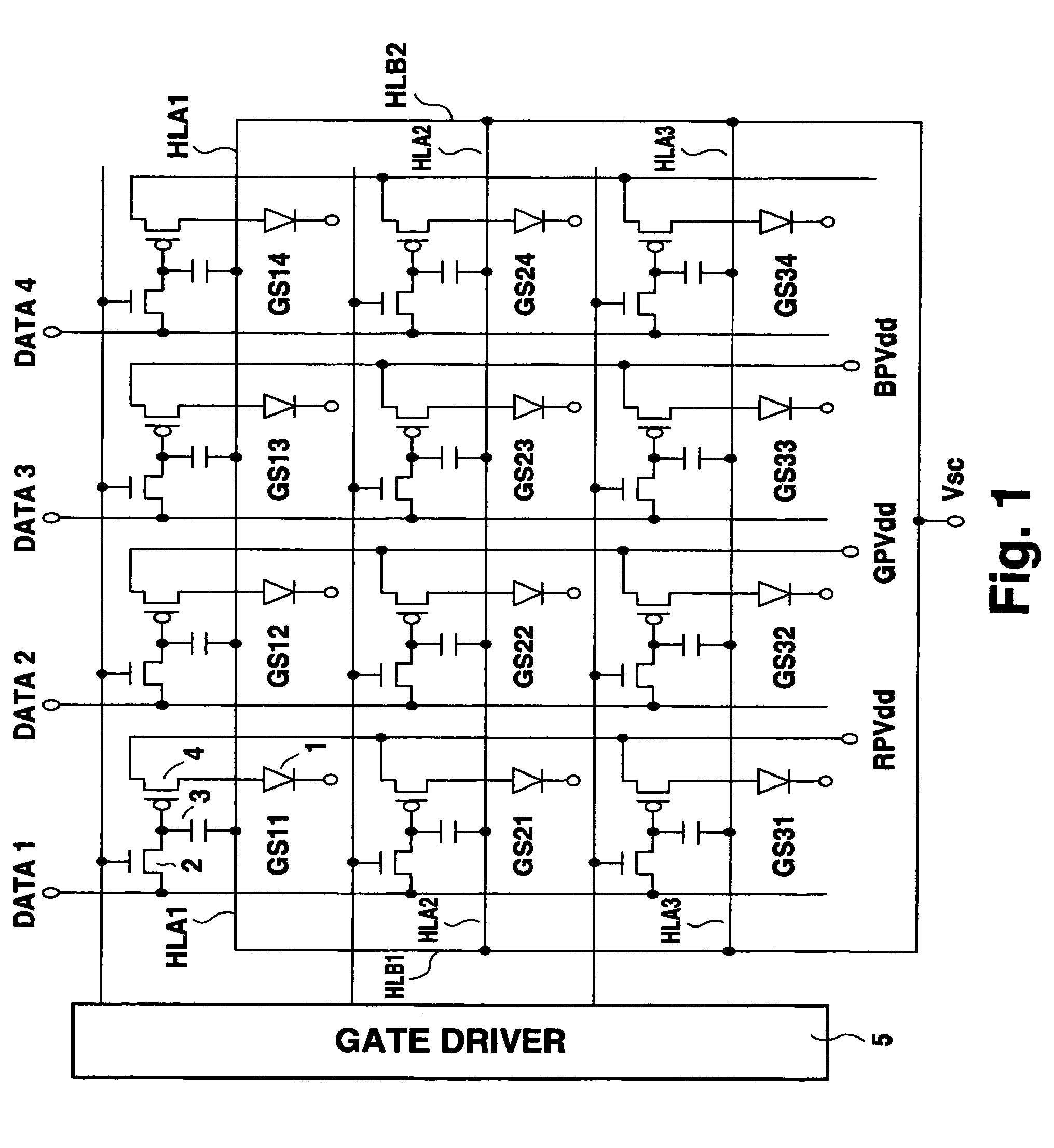
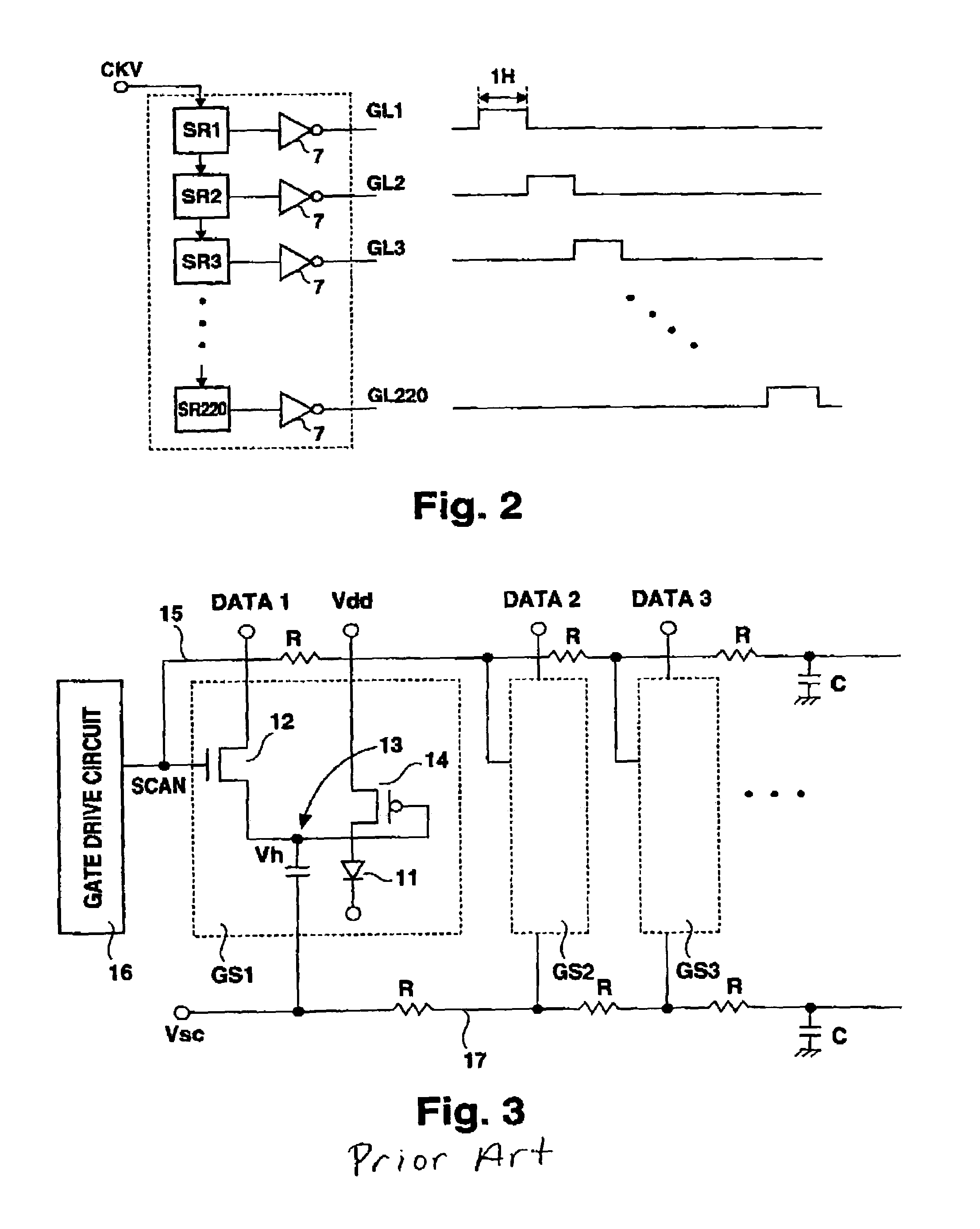
[0018]An active matrix type EL display device according to a preferred embodiment of the present invention is described hereinafter referring to FIGS. 1 and 2.

[0019]FIG. 1 is a circuit diagram schematically showing a structure of an active matrix type EL display device. Display pixels GS11, GS12, GS13, . . . GSij, are arranged in rows and columns to form a matrix. Each of the display pixels includes an organic EL element 1, a first thin film transistor 2 in which a display signal DATAj is applied to the drain and which is switched on and off in response to a select signal supplied from a gate signal line GLi, a capacitance 3, and a second thin film transistor 4 for driving the EL element 1 based on the display signal DATAj.

[0020]One end of the capacitance 3 is connected to the source of the first thin film transistor 2. The capacitance 3 is charged with a voltage corresponding to the display signal DATAj applied to the drain of the first thin film transistor and the voltage is maint...


PUM


Abstract

An active matrix type electroluminescence display device comprises a plurality of display pixels GS11, GS12, GS13, etc. arranged in a matrix of rows and columns, each display pixel including an EL element, a first thin film transistor in which a display signal is applied to the drain and which is switched on and off in response to a select signal, a capacitance with one end connected to the source of the first thin film transistor for maintaining a voltage corresponding to the display signal, and a second thin film transistor for driving the EL element based on the display signal. The other ends of the capacitance of row display pixels are connected to and shared by a plurality of first capacitance lines HLA1, HLA2, HLA3, HLAi. Both ends of the plurality of first capacitance lines HLA1, HLA2, HLA3 are connected to and shared by second capacitance lines HLB1 and HLB2. A constant voltage is supplied to the second capacitance line.

Description

BACKGROUND OF THE INVENTION[0001]1. Field of the Invention[0002]The present invention relates to an active matrix type EL display device with display pixels including an electroluminescence element (hereinafter referred to as an EL element) and a thin film transistor arranged in a matrix form, and particularly to an art for stably illuminating each display pixel by preventing voltage drops in capacitance lines connected to, and shared by, the display pixels.[0003]2. Description of the Related Art[0004]EL elements have various advantages, including, because they are self illuminating elements, an obviated need for a backlight as required in liquid crystal display devices and unlimited viewing angle. Because of these advantages, it is widely expected that EL elements will be use in the next generation of display devices.[0005]Two basic methods are known for driving EL elements. One of these is called a simple, or passive, matrix type, with the other, which employs a thin film transist...

Claims


Application Information

Patent Timeline
IPC IPC(8): G09G3/30G09F9/30H01L27/32H01L51/50H05B33/12H05B33/14H05B33/26H05B44/00
CPCG09G3/3225G09G3/3266H05B33/08Y02B20/325G09G2320/0223G09G2300/0842H05B33/26Y02B20/30
Inventor KOMIYA, NAOAKIOKUYAMA, MASAHIRO
Owner SANYO ELECTRIC CO LTD
Why Eureka
Try Eureka