Display apparatus, and image signal processing apparatus and drive control apparatus for the same

a technology of image signal processing and display apparatus, which is applied in the direction of instruments, computing, gearing, etc., can solve problems such as inability to carry ou

Inactive Publication Date: 2006-03-07
CANON KK
View PDF10 Cites 73 Cited by
  • Summary
  • Abstract
  • Description
  • Claims
  • Application Information

AI Technical Summary

Benefits of technology

[0011]Another purpose of the present invention is to provide a display apparatus which is able to calculate a current of a high voltage power supply (an anode current) and to carry out ABL precisely, and an image signal processing apparatus and a drive control apparatus for realizing the same.

Problems solved by technology

However, in case of the conventional compensation for voltage drop, the processing for limitation of electric power which is generally called ABL (Automatic Brightness Limiter) is not carried out.

Method used


Image

  • Display apparatus, and image signal processing apparatus and drive control apparatus for the same
  • Display apparatus, and image signal processing apparatus and drive control apparatus for the same
  • Display apparatus, and image signal processing apparatus and drive control apparatus for the same

Examples


first embodiment

[0105](First Embodiment)

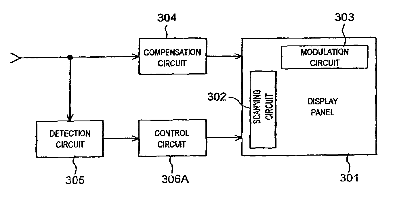
[0106]This embodiment relates to a display apparatus having a processing circuit for compensating an influence applied to a display image by voltage drop in a scanning wiring, in view of such a phenomenon that, in a display apparatus in which cold-cathode devices as the display devices are arranged in a simple matrix layout, the voltage drop occurs in electric current flowing into the scanning wiring and wiring resistance of the scanning wiring and a display image is deteriorated, and relates particularly to one which realizes it with relatively small circuit size.

[0107]The compensation circuit (voltage drop compensation circuit) for compensating the decrease of the applied voltage due to the voltage drop described here is one which calculates deterioration of the display image caused by the voltage drop in compliance with the input image data, and obtains the compensation data for compensating it, and applies the compensation to the image data.

[0108]In this ...

second embodiment

[0368](Second Embodiment)

[0369]A display apparatus according to a second embodiment of this invention which will be described later has a emission charge amount compensation unit for compensating change of the emission charge amount due to influence of the voltage drop, and, in an display apparatus in which the emission charge amount compensation unit calculates the compensated image data by compensating the input image data so as to correspond to the emission charge amount to be emitted, and the modulation unit outputs pulse wave forms which are applied to the column wiring according to the calculated compensated image data, is characterized by having a current value calculation unit for calculating an average current value corresponding to the light-emission luminance of the display apparatus based upon the integrated value of the input image data as a luminance desired value.

[0370]Or, also, it is characterized by having a compensated image data calculation unit which calculates t...

third embodiment

[0502](Third Embodiment)

[0503]In order to prevent the overflow, in the second embodiment, the maximum value of the compensated image data was detected, and in order for the maximum value to correspond to the maximum value of the input range of the modulation unit, the gain was calculated, and the gain was multiplied with the compensated image data, and thereby, the overflow was prevented.

[0504]In contrast to this, in a third embodiment, to detect the maximum value of the compensated image data is the same but, in order for the maximum value to correspond to the maximum value of the input range of the modulation unit, a value of the image data before the compensation is applied is made to be limited. That is, in order to prevent the overflow, the gain is multiplied with the image data which was inputted in advance to lessen its amplitude range, and thereby, the overflow is prevented.

[0505]Hereinafter, by use of FIG. 35, the overflow processing of this embodiment will be described.

[05...


PUM


Abstract

A display apparatus includes a display panel having display devices arranged in a matrix layout and driven through a plurality of row wirings and column wirings, a scanning unit to scan the row wirings, and a modulation unit to supply a modulation signal to the column wirings. A compensation unit applies compensation processing to compensate for fluctuation of display luminance due to the influence of voltage drop caused by a resistance of the row wiring to the image data, and a luminance control unit controls display luminance of the display panel based upon luminance information of the image data.

Description

BACKGROUND OF THE INVENTION[0001]1. Field of the Invention[0002]This invention relates to display apparatuses such as display apparatuses for televisions and computers for receiving television signals and image signals of computers etc. and displaying images, and image signal processing apparatuses and drive control apparatuses for them.[0003]More closely, it relates to a display apparatus which compensates a decreased portion of drive voltage resulting from electric resistance that a matrix wiring of a display panel has and effectively applied to display devices, and can drive the display devices with appropriate drive voltage, and an image signal processing apparatus and a drive control apparatus for the same.[0004]2. Description of the Related Art[0005]One of display devices is a cold cathode device. A example of a display apparatus having cold cathode devices is disclosed in JP Patent Publication No. 8-248920 (U.S. Pat. No. 5,734,361 specification). The display apparatus describ...

Claims


Application Information

Patent Timeline
Patent Type & Authority Patents(United States)
IPC IPC(8): G09G3/36G09G3/22G09G3/30G09G3/32
CPCG09G3/22G09G3/30G09G3/3208G09G2320/0223Y10T74/1888G09G2320/0285G09G2320/0626Y10T74/18568G09G2320/0276
Inventor ABE, NAOTOINAMURA, KOHEISAGANO, OSAMUSAITO, HIROSHIIKEDA, TAKESHI
Owner CANON KK
Why Eureka
Try Eureka