Semiconductor memory device and testing method thereof

a memory device and semiconductor technology, applied in the direction of information storage, static storage, digital storage, etc., can solve the problems of inability to use conventional testers without this capacity, inability to increase the speed of a dram core in proportion to an input and output signal rate, and the cost of manufacturing a semiconductor memory device can be reduced

Inactive Publication Date: 2009-07-28
LONGITUDE SEMICON S A R L
View PDF17 Cites 34 Cited by
  • Summary
  • Abstract
  • Description
  • Claims
  • Application Information

AI Technical Summary

Benefits of technology

[0007]It is another object of the present invention to provide a synchronous semiconductor memory device that can carry out a test using a low-speed tester.
[0011]A testing method of a semiconductor memory device according to the invention is used to test the semiconductor memory device mentioned above. According to this method, test data is continuously supplied to a serial-parallel conversion circuit synchronously with an external clock. Therefore, when test data having different logical values for each half cycle of an external clock are alternately supplied, test data having different logical values can be written into adjacent memory cells in the same mini array. With this arrangement, a pattern sensitivity test can be carried out correctly.
[0012]According to the present invention, a low-speed tester can be used to correctly test the operation of a semiconductor memory device that inputs and outputs data synchronously with a high-speed clock. Therefore, it is not necessary to develop a high-speed tester to match the operation speed of a semiconductor memory device. Consequently, the manufacturing cost of a semiconductor memory device can be reduced.

Problems solved by technology

While the speed of a clock used in a synchronous DRAM increases every year, the speed of a DRAM core cannot be increased in proportion to an input and output signal rate, because the DRAM core requires a precharge operation and a sense operation.
However, when the data transfer rate increases using the prefetch circuit, it also becomes necessary to use a high-speed tester to test the operation of the DRAM.
Therefore, a conventional tester that does not have this capacity cannot be used as it is.
Furthermore, because the operation test of a DRAM is carried out in a wafer state before dicing, a probe of a tester also becomes relatively large.
Therefore, a parasitic capacitance of the tester becomes larger than that of wiring actually used, and the speed of the tester cannot be increased easily.
These problems occur not only in the DRAM but also synchronous semiconductor memory devices in general.

Method used


Image

  • Semiconductor memory device and testing method thereof
  • Semiconductor memory device and testing method thereof
  • Semiconductor memory device and testing method thereof

Examples


Embodiment Construction

[0025]Preferred embodiments of the present invention will now be explained in detail with reference to the drawings.

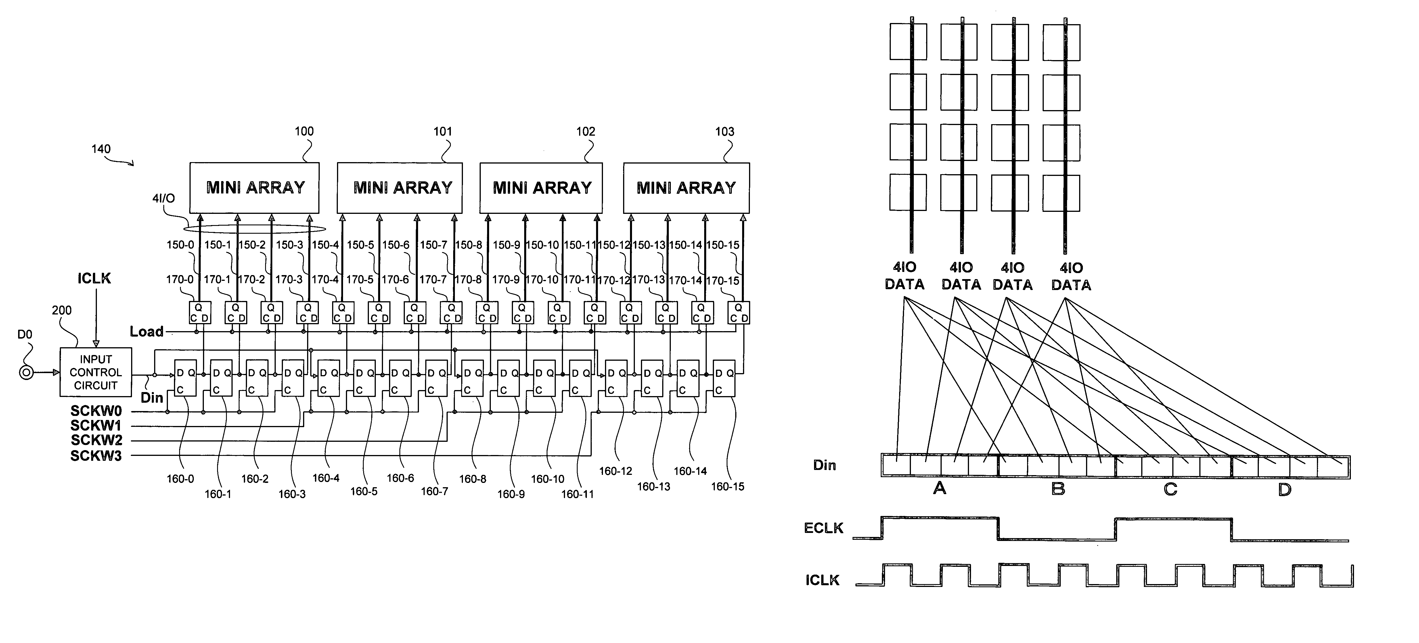
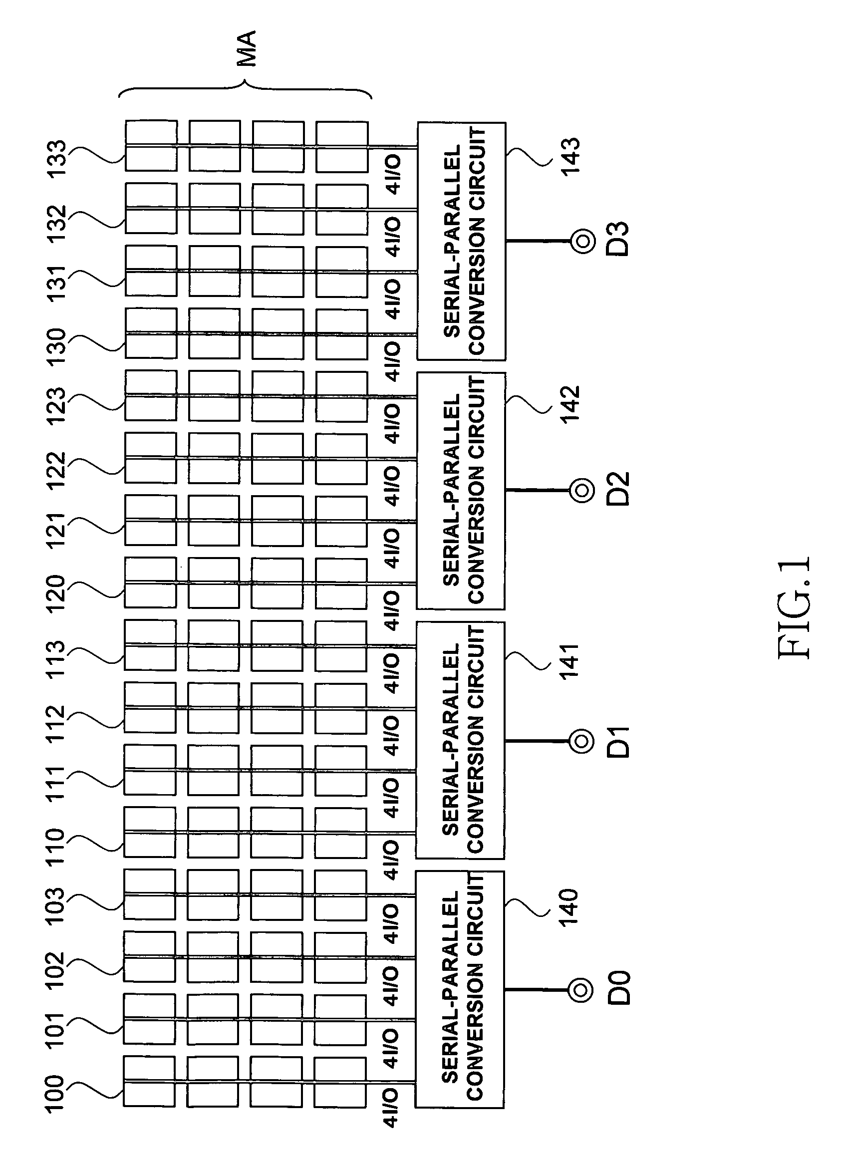
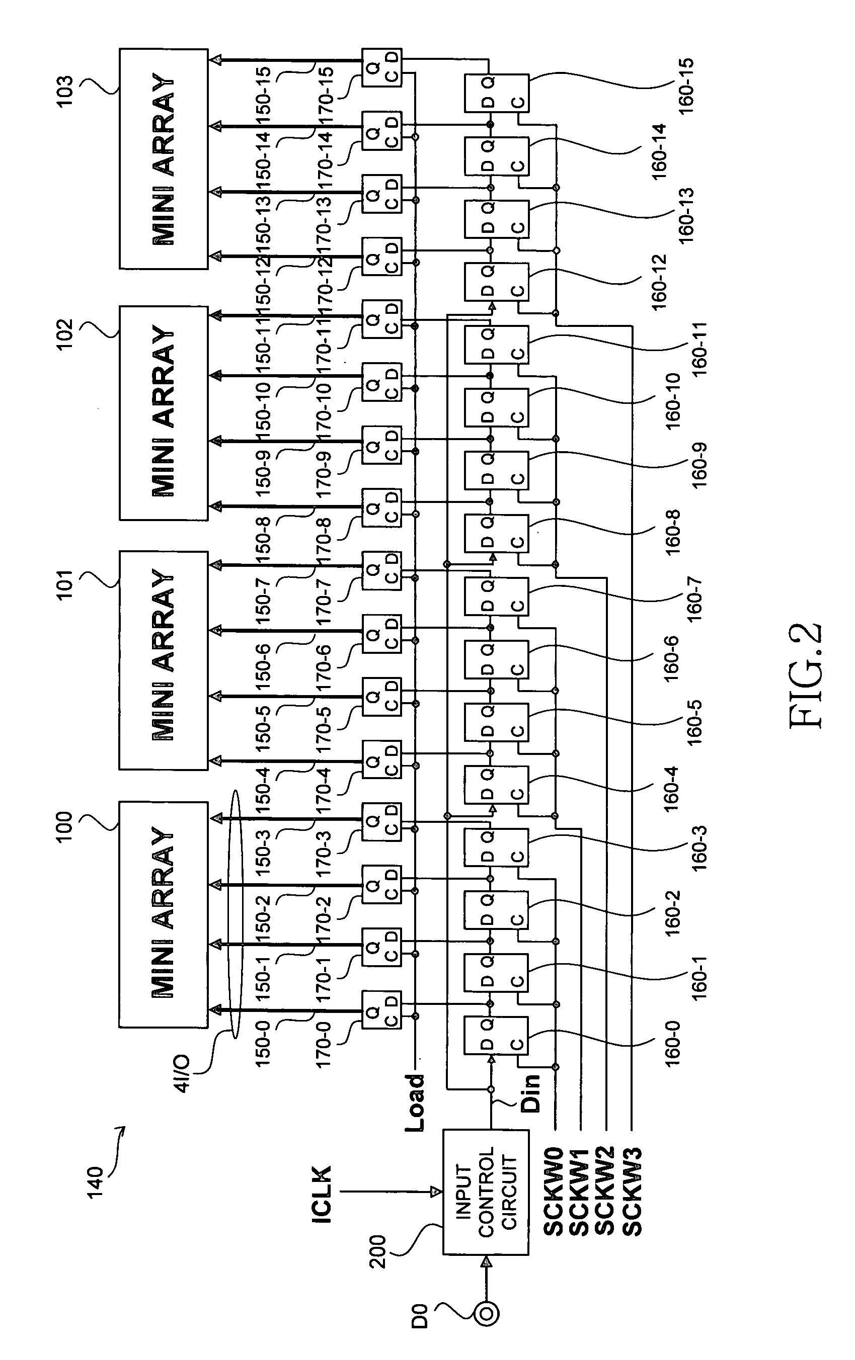
[0026]FIG. 1 is a schematic diagram of an entire configuration of a semiconductor memory device according to a preferred embodiment of the present invention.

[0027]The semiconductor memory device according to the present invention is a DRAM. As shown in FIG. 1, the semiconductor memory device includes a core region MA constituted by a plurality of mini arrays, data input and output pins D0 to D3, and serial-parallel conversion circuits 140 to 143 that are disposed between these data input and output pins and mini arrays.

[0028]The semiconductor memory device also includes various other elements necessary for the operation of the DRAM, such as various decoder circuits, precharge circuits, address pins, and command pins. However, these elements are not directly relevant to the scope of the invention, and are therefore omitted from the drawing.

[0029]The semiconductor memory...


PUM


Abstract

A semiconductor memory device includes mini arrays and a serial-parallel conversion circuit. The serial-parallel conversion circuit simultaneously writes two continuous data into mutually different mini arrays out of plural data that are continuously input synchronously with an internal clock, and continuously outputs two data simultaneously read from different mini arrays, synchronously with the internal clock. In testing the semiconductor memory device according to the present invention, one data is written during a period when an external clock having a cycle of an integer times cycle of the internal clock is fixed to a high level or a low level. With this arrangement, continuous data can be assigned to mutually different mini arrays.

Description

TECHNICAL FIELD[0001]The present invention relates to a semiconductor memory device and a testing method thereof. Particularly, the present invention relates to a synchronous semiconductor memory device that inputs and outputs data synchronously with a high-speed clock, and a testing method thereof.BACKGROUND OF THE INVENTION[0002]Conventionally, a synchronous DRAM (Dynamic Random Access Memory), that inputs and outputs data and a signal such as an address synchronously with a clock, is used in a wide range. While the speed of a clock used in a synchronous DRAM increases every year, the speed of a DRAM core cannot be increased in proportion to an input and output signal rate, because the DRAM core requires a precharge operation and a sense operation. Therefore, a synchronous DRAM has a “prefetch circuit” between a DRAM core and an input and output pin, and the prefetch circuit carries out a serial-parallel conversion, thereby achieving an apparent high-speed operation. See Patent La...

Claims


Application Information

Patent Timeline
Patent Type & Authority Patents(United States)
IPC IPC(8): G11C7/00
CPCG11C29/1201G11C29/32G11C29/26G11C2029/3202
Inventor ISHIKAWA, TORU
Owner LONGITUDE SEMICON S A R L
Why Eureka
Try Eureka