Method and apparatus for scanning, stitching, and damping measurements of a double-sided metrology inspection tool

a metrology inspection and double-sided technology, applied in the field of optical imaging, can solve the problems of small gaps, inaccurate measurements, etc., and achieve the effect of minimizing bending and stress

Inactive Publication Date: 2006-03-07
KLA TENCOR TECH CORP
View PDF18 Cites 21 Cited by
  • Summary
  • Abstract
  • Description
  • Claims
  • Application Information

AI Technical Summary

Benefits of technology

[0015]The present invention is a system for inspecting a wafer, including inspecting both sides of a dual sided wafer or specimen. The wafer is mounted using a fixed three point mounting arrangement which holds the wafer at a relatively fixed position while simultaneously minimizing bending and stress. Light energy is transmitted through a lensing arrangement employing lenses having diameter smaller than the specimen, such as half the size of the specimen, arranged to cause light energy to strike the surface of the wafer and subsequently pass through second collimating lens where detection and observation is performed.

Problems solved by technology

Smaller gaps provide problems when warped specimens are inspected.
The adjustability of the contact points provide the ability to hold the wafer without a stiff or hard connection, which could cause bending or deformation, as well as without a loose or insecure connection, which could cause inaccurate measurements.

Method used


Image

  • Method and apparatus for scanning, stitching, and damping measurements of a double-sided metrology inspection tool
  • Method and apparatus for scanning, stitching, and damping measurements of a double-sided metrology inspection tool
  • Method and apparatus for scanning, stitching, and damping measurements of a double-sided metrology inspection tool

Examples


Embodiment Construction

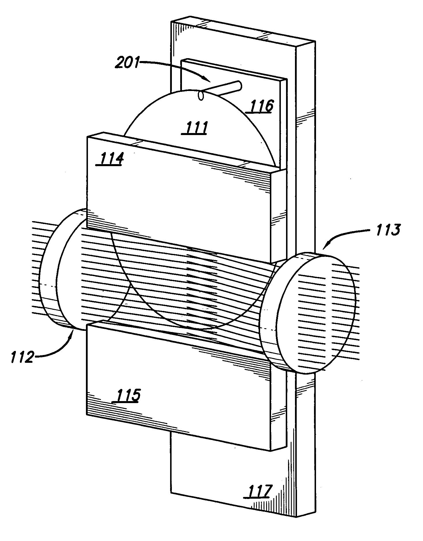
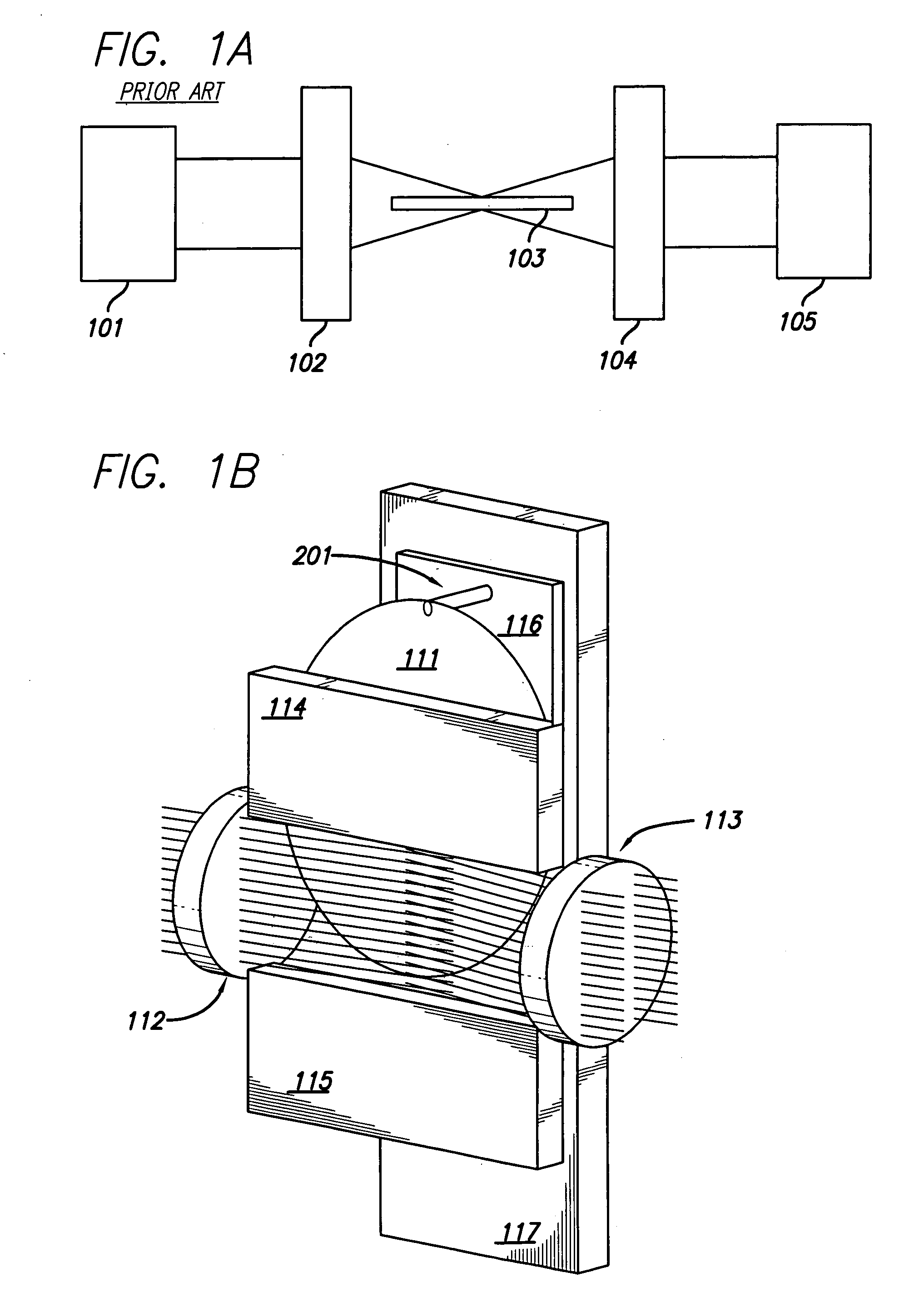
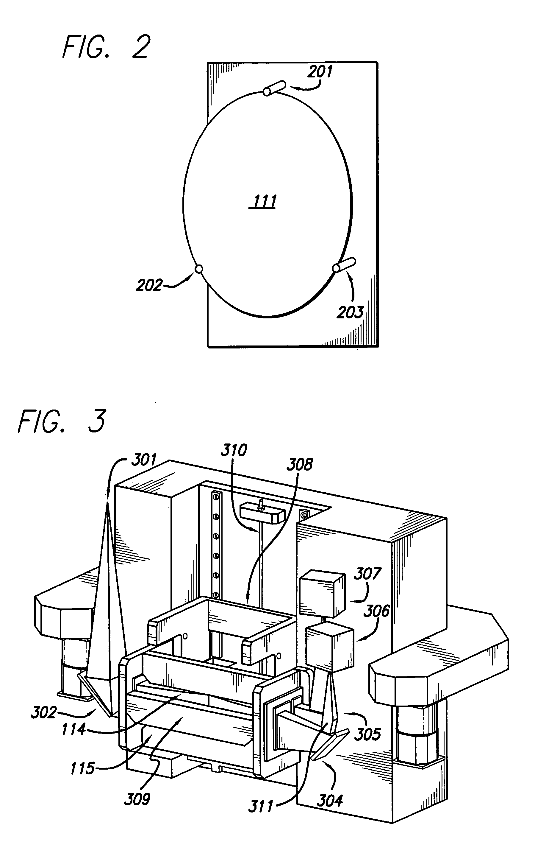
[0040]FIG. 1B illustrates a first embodiment of the present invention, specifically one for scanning both sides of a dual-sided wafer or specimen 111. According to FIG. 1B, the wafer 111 is mounted using a fixed three point mounting arrangement which is shown in FIG. 2. The three point mounting arrangement serves to hold the wafer 111 at a relatively fixed position while simultaneously minimizing any bending or stressing of the dual-sided wafer. Light energy is transmitted through first collimating lens 112 which is arranged to cause light energy to strike the surface of the wafer 111 and subsequently pass through second collimating lens 113 where detection and observation is performed. As may be appreciated by examining FIG. 1B, the diameter of both first collimating lens 112 and second collimating lens 113 are significantly smaller than the diameter of the specimen or wafer 111, and incident light strikes only a portion of the surface of wafer 111. Not shown in the illustration of...


PUM

PropertyMeasurementUnit
diametersaaaaaaaaaa
diametersaaaaaaaaaa
flatnessaaaaaaaaaa

Abstract

A system for inspecting specimens such as semiconductor wafers is provided. The system provides scanning of dual-sided specimens using a damping arrangement which filters unwanted acoustic and seismic vibration, including an optics arrangement which scans a first portion of the specimen and a translation or rotation arrangement for translating or rotating the specimen to a position where the optics arrangement can scan the remaining portion(s) of the specimen. The system further includes means for stitching the scans together, thereby providing both damping of the specimen and the need for smaller and less expensive optical elements.

Description

[0001]This application is a continuation of U.S. patent application Ser. No. 10 / 165,344, filed Jun. 7, 2002, now U.S. Pat. No. 6,686,996 entitled “Method and Apparatus for Scanning, Stitching, and Damping Measurements of a Double Sided Metrology Inspection Tool,” inventors Paul J. Sullivan, et al., which is a continuation of co-pending U.S. patent application Ser. No. 09 / 335,673, filed Jun. 18, 1999, entitled “Method and Apparatus for Scanning, Stitching, and Damping Measurements of a Double Sided Metrology Inspection Tool,” inventors Paul J. Sullivan, et al., now U.S. Pat. No. 6,414,752, issued Jul. 2, 2002.BACKGROUND OF THE INVENTION[0002]1. Field of the Invention[0003]The present invention relates generally to the field of optical imaging and more particularly to systems for sub-aperture data imaging of double sided interferometric specimens, such as semiconductor wafers.[0004]2. Description of the Related Art[0005]The progress of the semiconductor industry over the last years ha...

Claims


Application Information

Patent Timeline
Patent Type & Authority Patents(United States)
IPC IPC(8): G01N21/84G01B11/30G01N21/95G01R31/265G01R31/28H01L21/66
CPCG01N21/9501G01R31/2831G01R31/2656
Inventor SULLIVAN, PAUL J.KREN, GEORGESMEDT, RODNEY C.HANSEN, HANS J.SHORTT, DAVID W.KAVALDJIEV, DANIEL IVANOVBEVIS, CHRISTOPHER F.
Owner KLA TENCOR TECH CORP
Why Eureka
Try Eureka