Flip chip package capable of measuring bond line thickness of thermal interface material

a technology of thermal interface material and flip chip, which is applied in the direction of electrical equipment, semiconductor devices, semiconductor/solid-state device details, etc., can solve the problems of very limited sampling, high cost, and serious heat generation of flip chip, and achieve the effect of reducing any possible warpage of the heat sink

Active Publication Date: 2006-03-21
ADVANCED SEMICON ENG INC
View PDF8 Cites 39 Cited by
  • Summary
  • Abstract
  • Description
  • Claims
  • Application Information

AI Technical Summary

Benefits of technology

[0004]The second purpose of the present invention is to provide a flip chip package capable of measuring the bond line thickness (BLT) of the thermal interface material. A heat sink having an opening is attached to a flip chip. The back surface of the flip chip includes a region uncovered by the thermal interface material, which may includes an edge or a corner of the back surface. The opening exposes the uncovered region of the back surface. Therefore, the thickness distribution of the thermal interface material can be easily observed.
[0006]The fourth purpose of the present invention is to provide a flip chip package capable of measuring the bond line thickness (BLT) of the thermal interface material. The heat sink has at least an opening corresponding to the edge or the corner of the back surface of the flip chip to reduce any possible warpage of the heat sink.

Problems solved by technology

However, the heat generated from the flip chip becomes a serious problem in high-speed operation.
Under this kind of destructive measurement, the sampling is very limited and very time-consuming.

Method used


Image

  • Flip chip package capable of measuring bond line thickness of thermal interface material
  • Flip chip package capable of measuring bond line thickness of thermal interface material
  • Flip chip package capable of measuring bond line thickness of thermal interface material

Examples


first embodiment

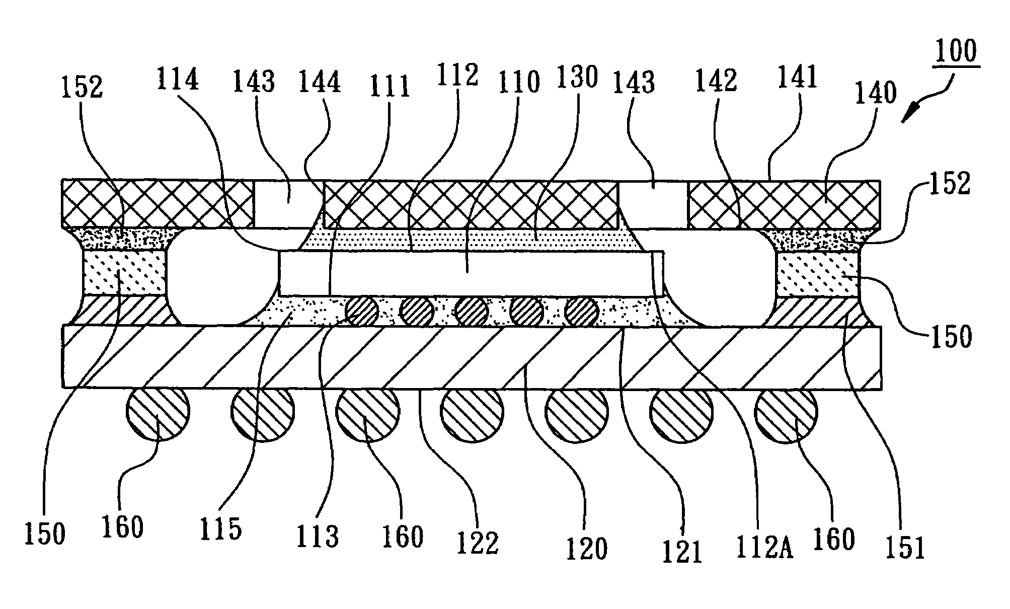
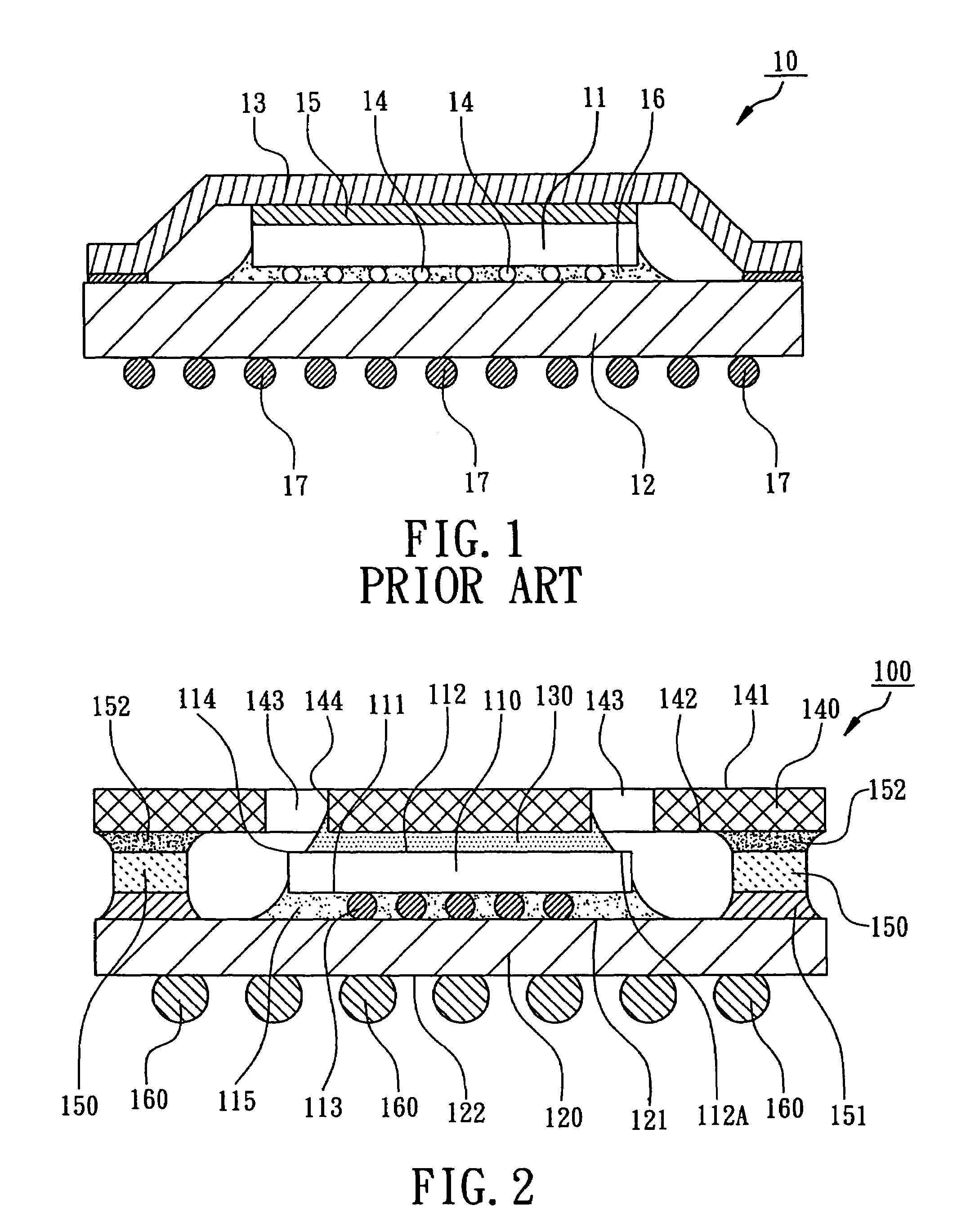
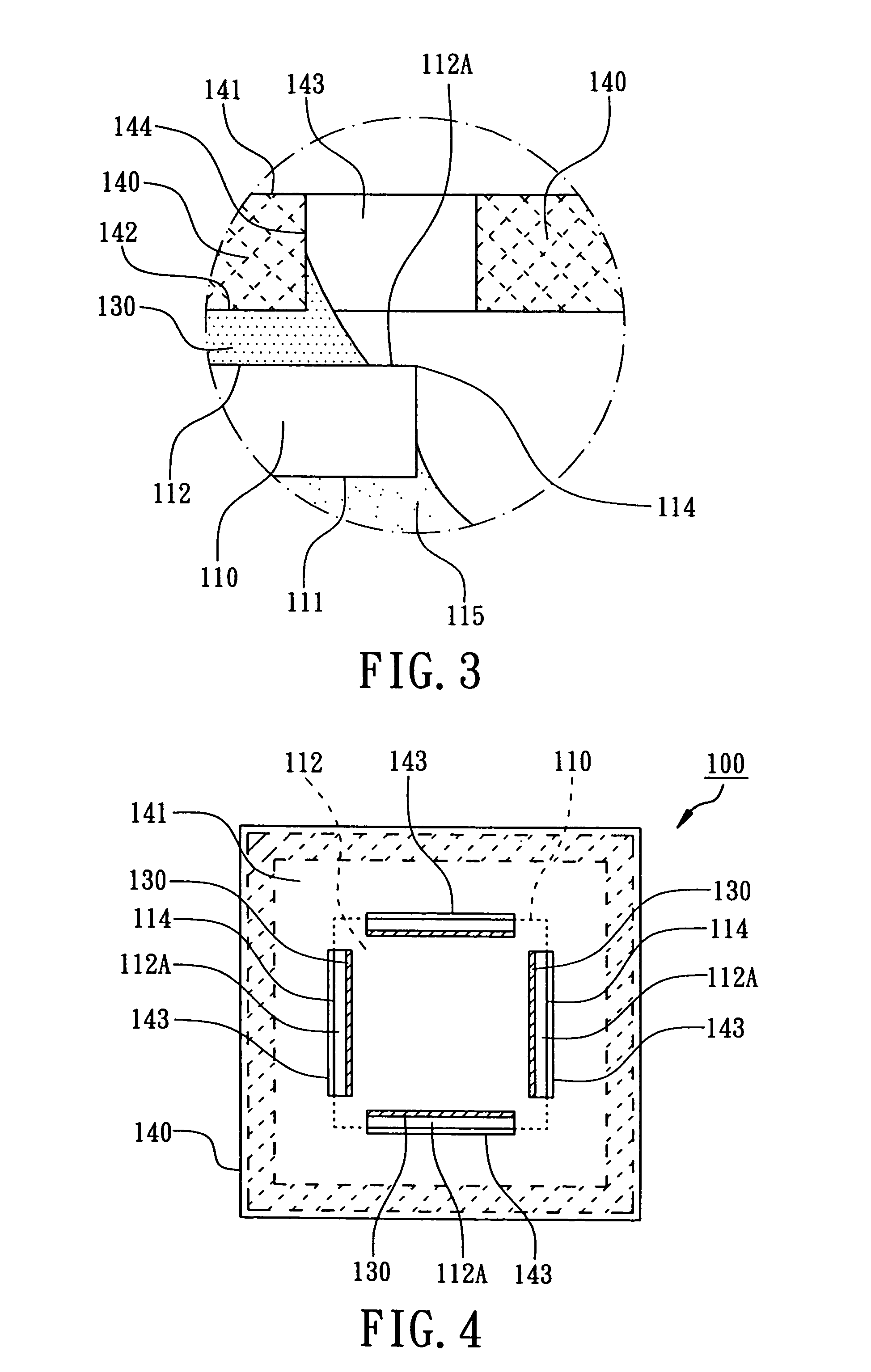
[0014]FIGS. 2, 3, and 4 show a flip chip package 100 capable of measuring the bond line thickness according to the present invention. The flip chip package 100 comprises a flip chip 110, a substrate 120, a thermal interface material 130, and a heat sink 140. The substrate 120 has an upper surface 121 and a lower surface 122. The substrate 120 has a plurality of flip-chip pads on the upper surface 121 for flip-chip bonding the flip chip 110. The flip chip 110 has an active surface 111 and a back surface 112. A plurality of bumps 113 are formed on the active surface 111. The back surface 112 includes a plurality of edges 114 and a plurality of corners between the edges 114. The flip chip 110 is mounted on the upper surface 121 of the substrate 120 via the bumps 113. Preferably, there is an underfilling material 115 applied between the active surface 111 of the flip chip 110 and the upper surface 121 of the substrate 120 to reduce the stress on the bumps 113.

[0015]The thermal interface...

second embodiment

[0018]In the present invention, FIG. 5 shows a flip chip package 200 capable of measuring the thickness of the thermal interface material. It comprises a flip chip 210, a substrate 220, a thermal interface material 230, and a heat sink 240. The flip chip 210 has an active surface 211 and a back surface 212. The flip chip 210 is mounted on the active surface 221 of the substrate 220 via a plurality of bumps 213. The thermal interface material 230 is dispensed on the back surface 212 of the flip chip 210. The heat sink 240 has a first surface 241, a second surface 242 and at least an opening 243 passing through the first surface 214 and the second surface 242. And the second surface 242 of the heat sink 240 is attached to the thermal interface material 230. Furthermore, the back surface 212 of the flip chip 210 includes a region 212A uncovered from the thermal interface material 230, also the uncover region 212A is exposed out of the opening 243 of the heat sink 240. In this embodimen...

third embodiment

[0019]In the present invention, FIG. 6 shows a flip chip package 300 capable of measuring the thickness of the thermal interface material. The package 300 comprises a flip chip 310, a substrate 320, a thermal interface material 330, and a heat sink 340. The flip chip 310 has an active surface 311 and a back surface 312. The flip chip 310 is mounted on the active surface 321 of the substrate 320 via the bumps 313. The heat sink 340 has a first surface 341, a second surface 342 and at least an opening 343 passing through the first surface 314 and the second surface 342. The thermal interface material 330 is applied between the back surface 312 of the flip chip 310 and the second surface 342 of the heat sink 340. The back surface 312 of the flip chip 310 includes a region 312A uncovered from the thermal interface material 330, also the uncovered region 312A is exposed out of the opening 343 of the heat sink 340. The uncovered region 312A enables to be measured to obtain Z-axis height o...


PUM


Abstract

A flip chip package includes a substrate, a flip chip, a thermal interface material and a heat sink. The flip chip is mounted on the substrate. The thermal interface material is applied on the back surface of the flip chip. The back surface of the flip chip includes a region uncovered by the thermal interface material. The opening exposes the uncover region of the back surface of the flip chip for measuring the height of the back surface. Also the opening has an inner sidewall above the back surface for fillet bonding of the thermal interface material. Therefore the bond line thickness (BLT) of the thermal interface material can be measured and calculated.

Description

FIELD OF THE INVENTION[0001]The present invention relates to a flip chip package, and in particular to a flip chip package capable of measuring the bond line thickness (BLT) of thermal interface material between a heat sink and a flip chip, also capable of observing the distribution of the thermal interface material on the back surface of the flip chip.BACKGROUND OF THE INVENTION[0002]It is well known that the flip chip package is lighter, thinner, shorter, and smaller than other packages. Furthermore, the flip chip package includes a flip chip which is flip-chip mounted on a substrate via bumps so that the signal path from the flip chip to the substrate becomes shorter for high-speed applications. However, the heat generated from the flip chip becomes a serious problem in high-speed operation. Therefore, it is important to solve the heat dissipation problem in a flip chip package. R.O.C. Taiwan Patent No. 508,778 entitled “Package structure of semiconductor chip” discloses a conven...

Claims


Application Information

Patent Timeline
Patent Type & Authority Patents(United States)
IPC IPC(8): H01L23/10H01L23/34
CPCH01L23/3675H01L23/36H01L23/3672H01L2224/73253H01L2224/16225H01L2924/16152H01L2924/16195H01L2924/15311H01L2224/32225H01L2224/32245H01L2224/33181H01L2224/73204H01L2224/83385H01L2924/16151H01L2924/16251H01L2924/00014H01L2924/00011H01L2924/00H01L2224/0401
Inventor WANG, SUNG-FEI
Owner ADVANCED SEMICON ENG INC
Why Eureka
Try Eureka