Liquid crystal display having undulated anisotropic reflection electrodes and openings therein
a liquid crystal display and anisotropic reflection technology, applied in the field of semi-transmission liquid crystal display, can solve the problems of inability to form color filters with different thicknesses on the opposite substrate for different areas, drop in luminance, and difficulty in forming color filters with different thicknesses on the opposite substrate, etc., to achieve the effect of enhancing the output light intensity of the liquid crystal display
- Summary
- Abstract
- Description
- Claims
- Application Information
AI Technical Summary
Benefits of technology
Problems solved by technology
Method used
Image
Examples
first embodiment
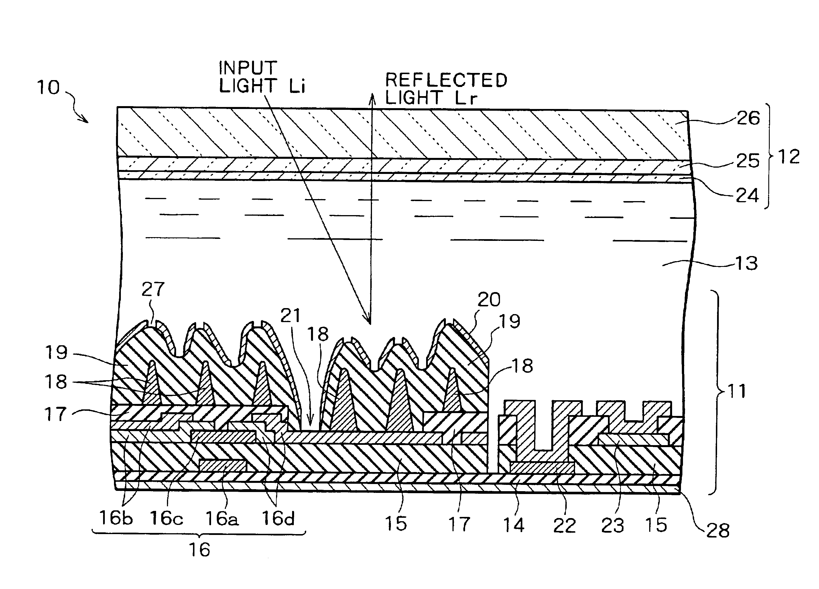
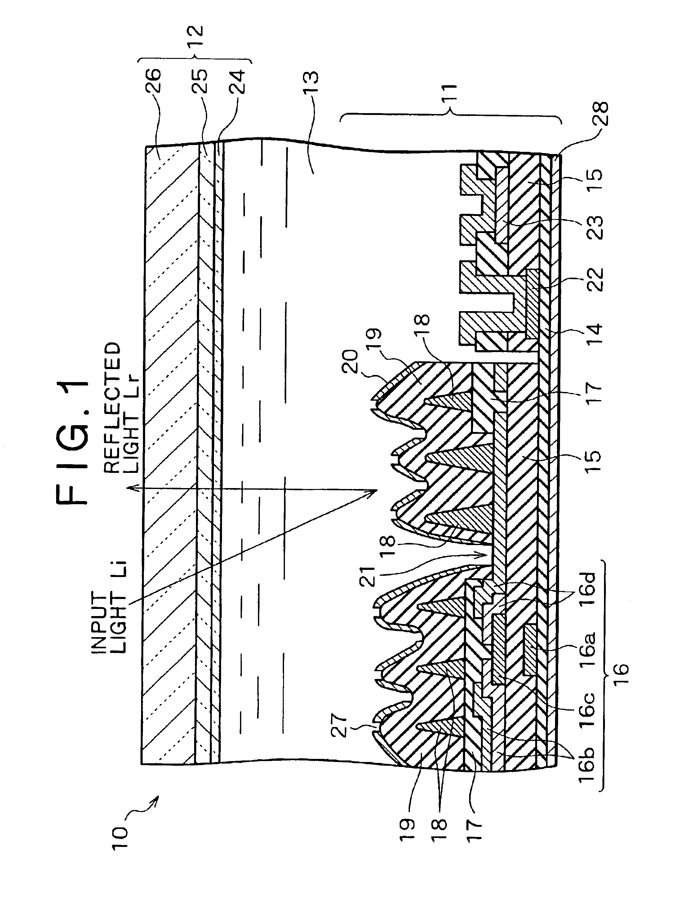
[0094]Embodiments of the invention will be described below with reference to the accompanying drawings. FIG. 1 is a partial cross-sectional view of a semi-transmission type liquid crystal display according to the present invention. As shown in FIG. 1, a semi-transmission type liquid crystal display 10 has, inside, a lower substrate 11, an opposite substrate 12 so arranged as to face the lower substrate 11 and a liquid crystal layer 13 sandwiched between the lower substrate 11 and the opposite substrate 12.
[0095]The semi-transmission type liquid crystal display 10 employs an active matrix system which has, for example, thin film transistors (TFTs) provided as switching elements pixel by pixel.
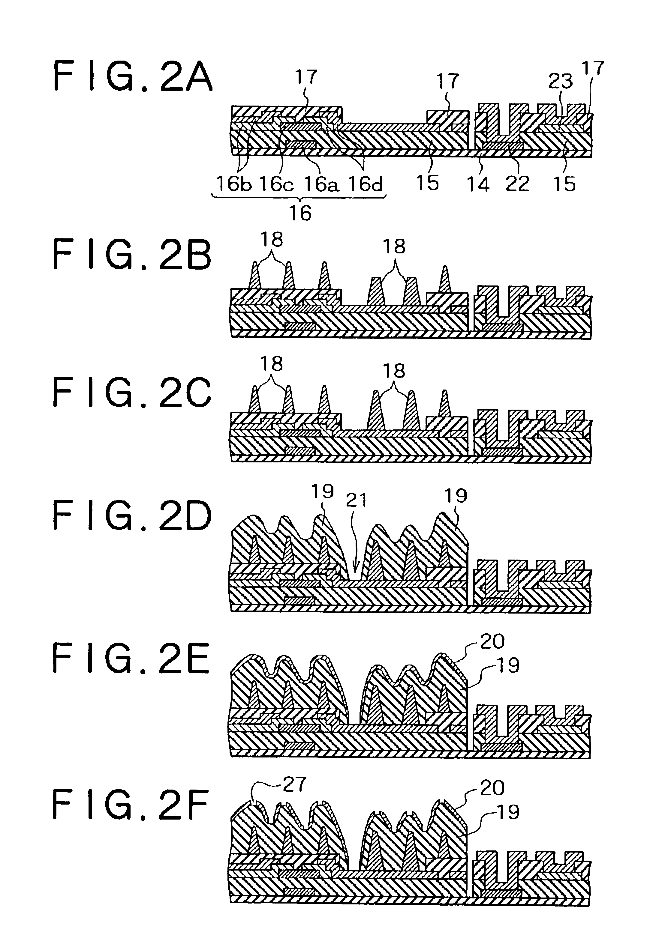
[0096]The lower substrate 11 has an insulative substrate 14, an insulating protection film 15, TFTs 16, an insulating layer 17, projection patterns 18, a second insulating layer 19 and a reflection electrode 20. The insulating protection film 15 is deposited on the insulative substrate 14 and th...
second embodiment
[0131]FIG. 14 is a partial cross-sectional view of a semi-transmission type liquid crystal display according to the invention. As shown in FIG. 14, a semi-transmission type liquid crystal display 10 has, inside, a lower substrate 11, an opposite substrate 12 so arranged as to face the lower substrate 11 and a liquid crystal layer 13 sandwiched between the lower substrate 11 and the opposite substrate 12.
[0132]The lower substrate 11 has an insulative substrate 14, an insulating protection film 15, TFTs 16, an insulating layer 17, projection patterns 18, a second insulating layer 19, a reflection electrode 20 and a transparent electrode 31. The insulating protection film 15 is deposited on the insulative substrate 14 and the TFTs 16 are formed on the insulating protection film 15. Each TFT 16 has a gate electrode 16a on the insulative substrate 14, a drain electrode 16b, a semiconductor layer 16c and a source electrode 16d, the last three electrodes lying on the insulating protection ...
third embodiment
[0159]In the display of the reflection mode, input light from the opposite substrate 12 passes the color filter 25 provided on the opposite substrate 12 twice until it becomes output light, In the display of the transmission mode, the light from the backlight 28 passes the color filter 25 provided on the lower substrate 11 and the color filter 25 provided on the opposite substrate 12 until it becomes output light. In reflection and transmission modes, the light passes the color filter twice, so that the liquid crystal display of the third embodiment can make the color expression identical in both modes. It is also possible to determine the balance of colors displayed independently between the transmission mode and reflection mode.
[0160]An ECB (Electrically Controlled Birefringence) type, homogeneous type, homeotropic type, TN type, HAN type, OCB type or the like is used for the liquid crystal layers 13 according to the first embodiment and the second embodiment.
[0161]FIGS. 18A throu...
PUM
| Property | Measurement | Unit |
|---|---|---|
| polar angle | aaaaa | aaaaa |
| tilt angle | aaaaa | aaaaa |
| tilt angle | aaaaa | aaaaa |
Abstract
Description
Claims
Application Information


