Method of forming isolation film in semiconductor device

Inactive Publication Date: 2006-03-28
SK HYNIX INC
View PDF12 Cites 6 Cited by
  • Summary
  • Abstract
  • Description
  • Claims
  • Application Information

AI Technical Summary

Benefits of technology

[0009]Accordingly, the present invention has been made in view of the above problems, and it is an object of the present invention to provide a method of forming isolation films of semiconductor devices, wherein plasma damages generated in a process of forming the isolation film can be prevented.
[0010]Another object of the present invention is to provide a method of forming isolation films of semiconductor devices, wherein moat fail generated in the isolation films can be prevented.
[0015]The predetermined depth of the patterned semiconductor substrate can be a depth that causes the first insulating film for trench burial to be easily buried in the trenches.

Problems solved by technology

As the depth of the isolation film increases due to reduction of a pattern space even through the STI process, however, void, etc. is generated in insulation films buried in trenches.
As plasma is used upon etching, there is a problem in that plasma damages are generated in the semiconductor substrate that will be defined as the active region.
Furthermore, as plasma is used in a deposition process of the insulation film, there is also a problem in that plasma damages are generated.
In this case, there is a problem in that moat fail is generated in top corners of the isolation film due to the sidewall oxide films.

Method used


Image

  • Method of forming isolation film in semiconductor device
  • Method of forming isolation film in semiconductor device
  • Method of forming isolation film in semiconductor device

Examples


Embodiment Construction

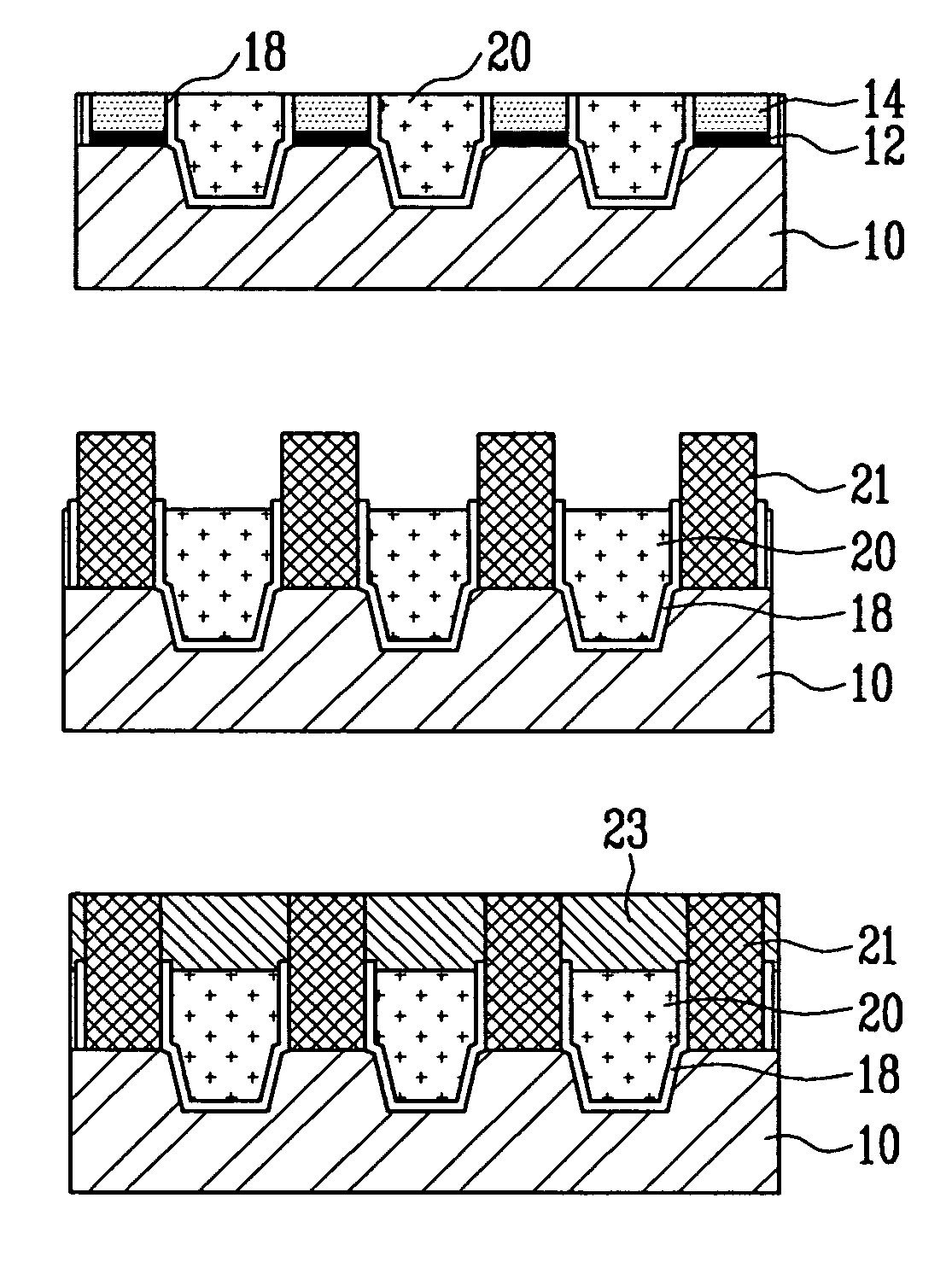
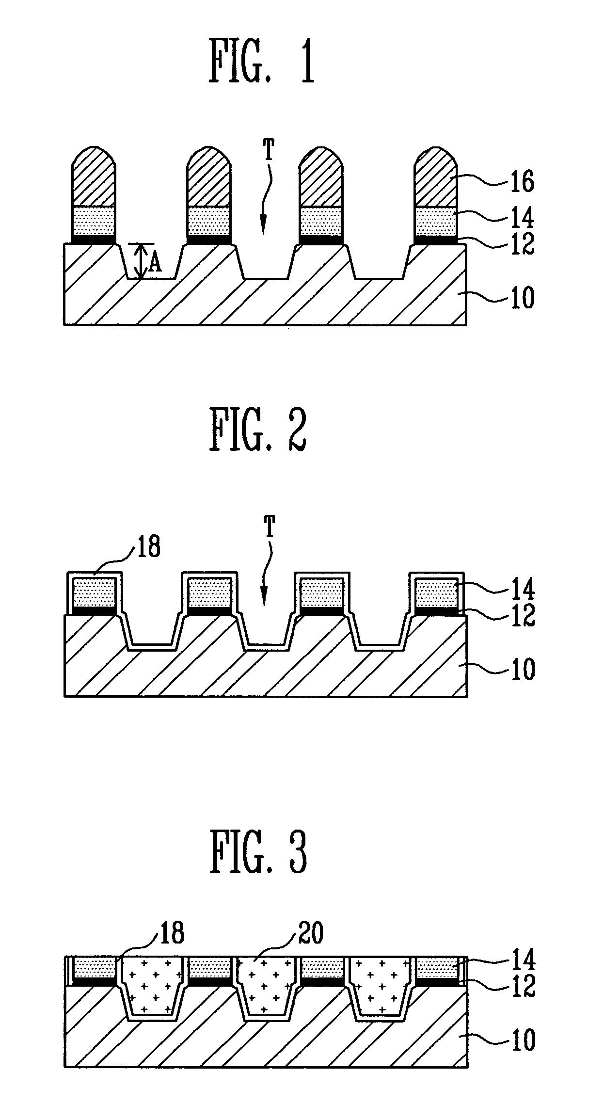
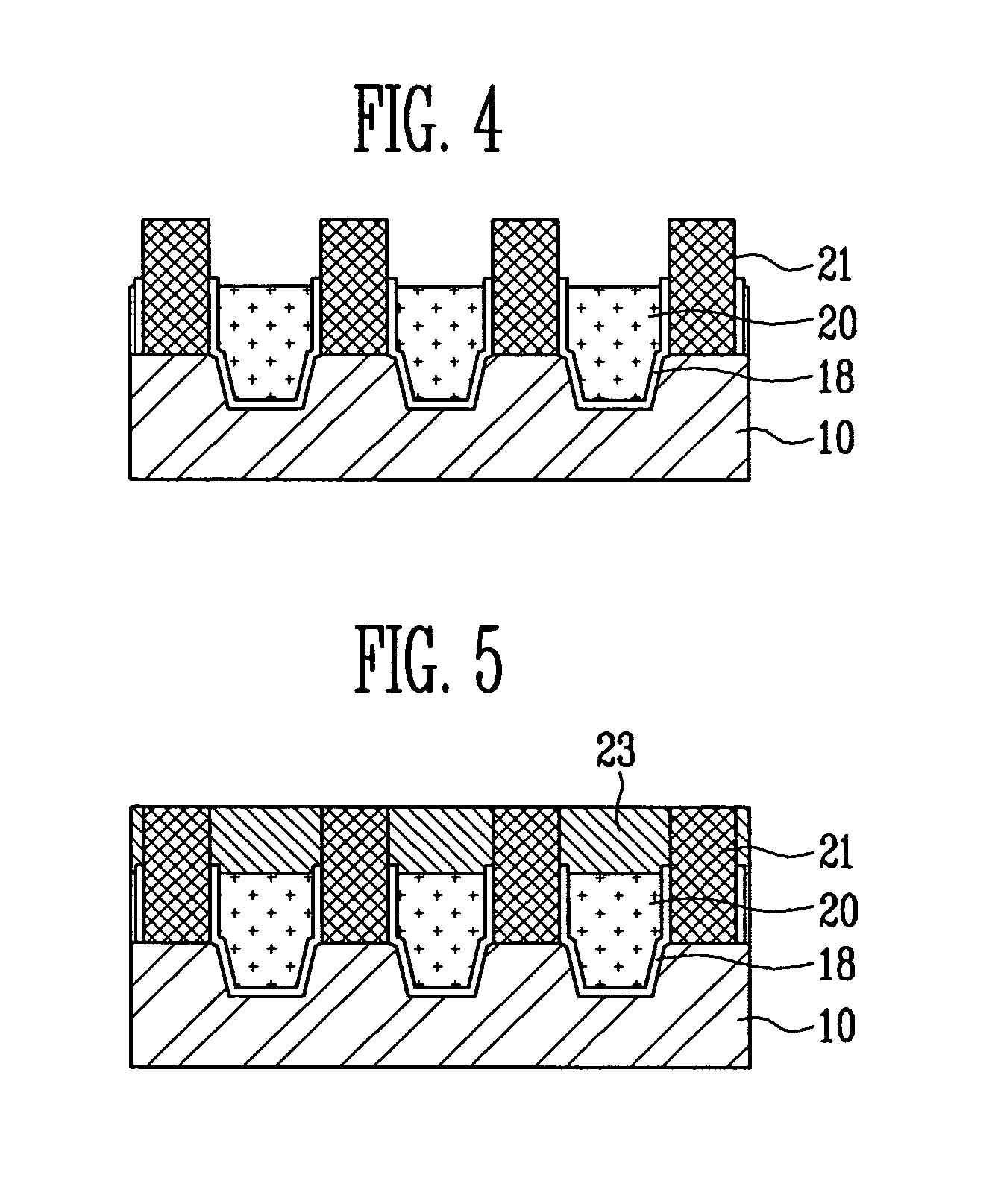
[0020]Now, the preferred embodiments according to the present invention will be described with reference to the accompanying drawings. Since preferred embodiments are provided for the purpose that the ordinary skilled in the art are able to understand the present invention, they may be modified in various manners and the scope of the present invention is not limited by the preferred embodiments described later. Meanwhile, in case where it is described that one film is “on” the other film or a semiconductor substrate, the one film may directly contact the other film or the semiconductor substrate. Or, a third film may be intervened between the one film and the other film or the semiconductor substrate. Furthermore, in the drawing, the thickness and size of each layer are exaggerated for convenience of explanation and clarity. Like reference numerals are used to identify the same or similar parts.

[0021]FIGS. 1 to 5 are cross-sectional views for explaining a method of forming an isolat...


PUM


Abstract

The present invention relates to a method of forming an isolation film of a semiconductor device. According to the present invention, the method includes the steps of forming a pad film on a semiconductor substrate, and patterning the pad film of a predetermined region and a predetermined depth of the semiconductor substrate to form trenches, forming sidewall oxide films on sidewalls of the trenches thereby defining a non-active region and an active region, forming a first oxide film for trench burial on the entire surface including the sidewall oxide films, and then performing a polishing process until the pad film is exposed, thus forming a first isolation film, removing the pad film to expose the semiconductor substrate in the active region, forming a silicon layer, which has a height higher than that of the first isolation film, on the exposed semiconductor substrate in the active region, and forming a second oxide film for trench burial on the entire surface, and then performing a polishing process until the silicon layer is exposed, thus forming a second isolation film, whereby an isolation film in which the first isolation film and the second isolation film are stacked is formed.

Description

BACKGROUND[0001]1. Field of the Invention[0002]The present invention relates to a method of manufacturing semiconductor devices, and more specifically, to a method of forming isolation films of semiconductor devices.[0003]2. Discussion of Related Art[0004]In a method of manufacturing semiconductor devices, an isolation film for separately defining an active region and a non-active region is formed. Recently, as semiconductor device becomes higher integrated and dense, a STI (Shallow Trench Isolation) process has been employed.[0005]As the depth of the isolation film increases due to reduction of a pattern space even through the STI process, however, void, etc. is generated in insulation films buried in trenches.[0006]Further, when the isolation film is formed by means of the STI process, the semiconductor substrate is etched to form the trench. As plasma is used upon etching, there is a problem in that plasma damages are generated in the semiconductor substrate that will be defined ...

Claims


Application Information

Patent Timeline
IPC IPC(8): H01L21/762
CPCH01L21/76224H01L21/762
Inventor YANG, YOUNG HO
Owner SK HYNIX INC
Why Eureka
Try Eureka