Method of forming a selectively converted inter-layer dielectric using a porogen material

a technology of porogen material and inter-layer dielectric, which is applied in the direction of basic electric elements, electrical equipment, semiconductor devices, etc., can solve the problems of poor strength, low fracture toughness, inferior mechanical properties,

Inactive Publication Date: 2006-03-28
INTEL CORP
View PDF8 Cites 79 Cited by
  • Summary
  • Abstract
  • Description
  • Claims
  • Application Information

AI Technical Summary

Problems solved by technology

Although such materials may serve to lower the dielectric constant, they may offer inferior mechanical properties such as poor strength and low fracture toughness.
One major issue facing low-k void technology is how to remove sacrificial material to facilitate multi-layer structures.
Another major issue facing low-k void technology is how to facilitate void creation while providing a structure which can withstand conventional processing treatments, such as chemical-mechanical polishing and thermal treatment, as well as post processing mechanical and thermo-mechanical rigors.

Method used


Image

  • Method of forming a selectively converted inter-layer dielectric using a porogen material
  • Method of forming a selectively converted inter-layer dielectric using a porogen material
  • Method of forming a selectively converted inter-layer dielectric using a porogen material

Examples


Embodiment Construction

[0006]In the following detailed description of embodiments of the invention, reference is made to the accompanying drawings in which like references indicate similar elements. The illustrative embodiments described herein are disclosed in sufficient detail to enable those skilled in the art to practice the invention. The following detailed description is therefore not to be taken in a limiting sense, and the scope of the invention is defined only by the appended claims.

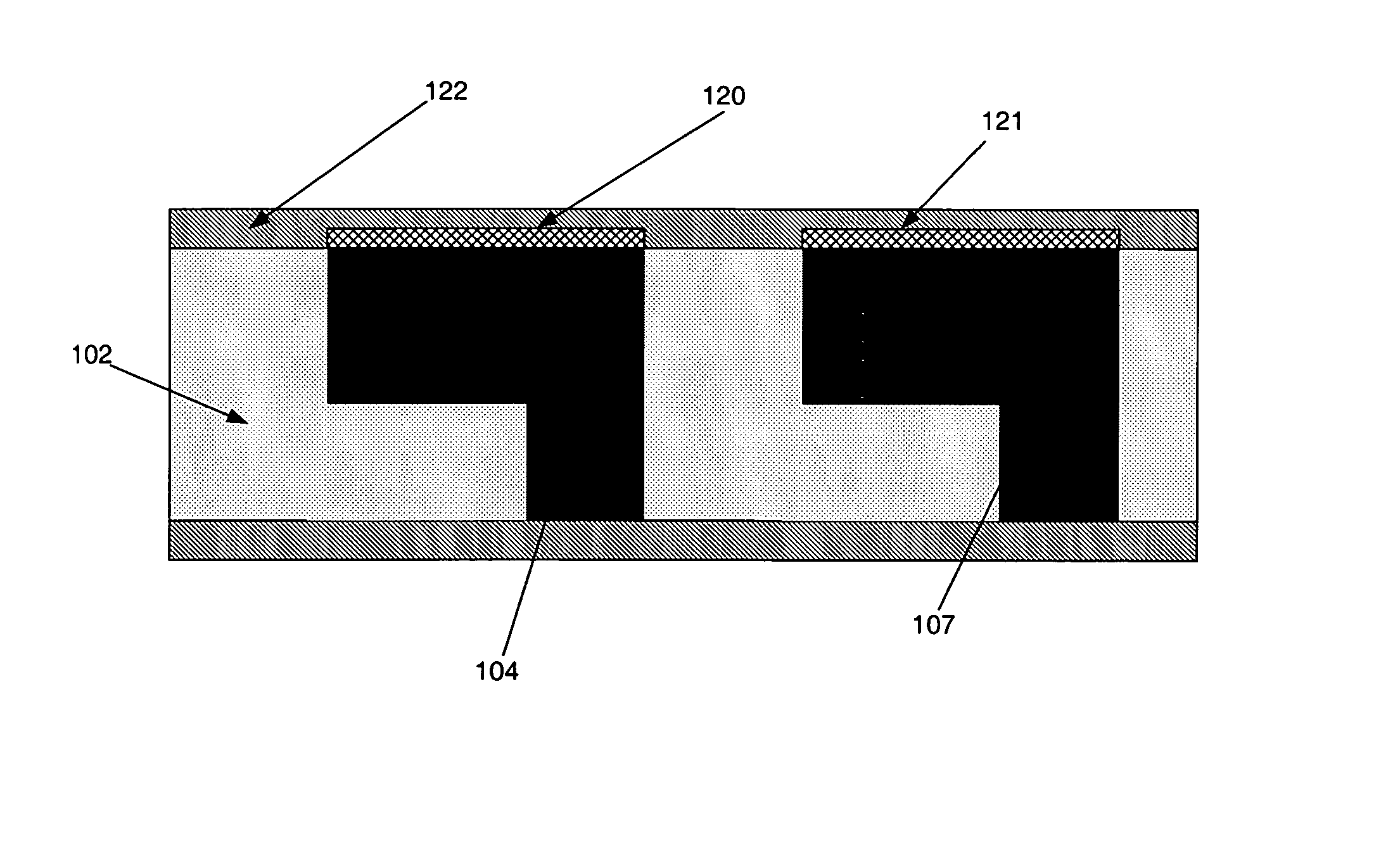
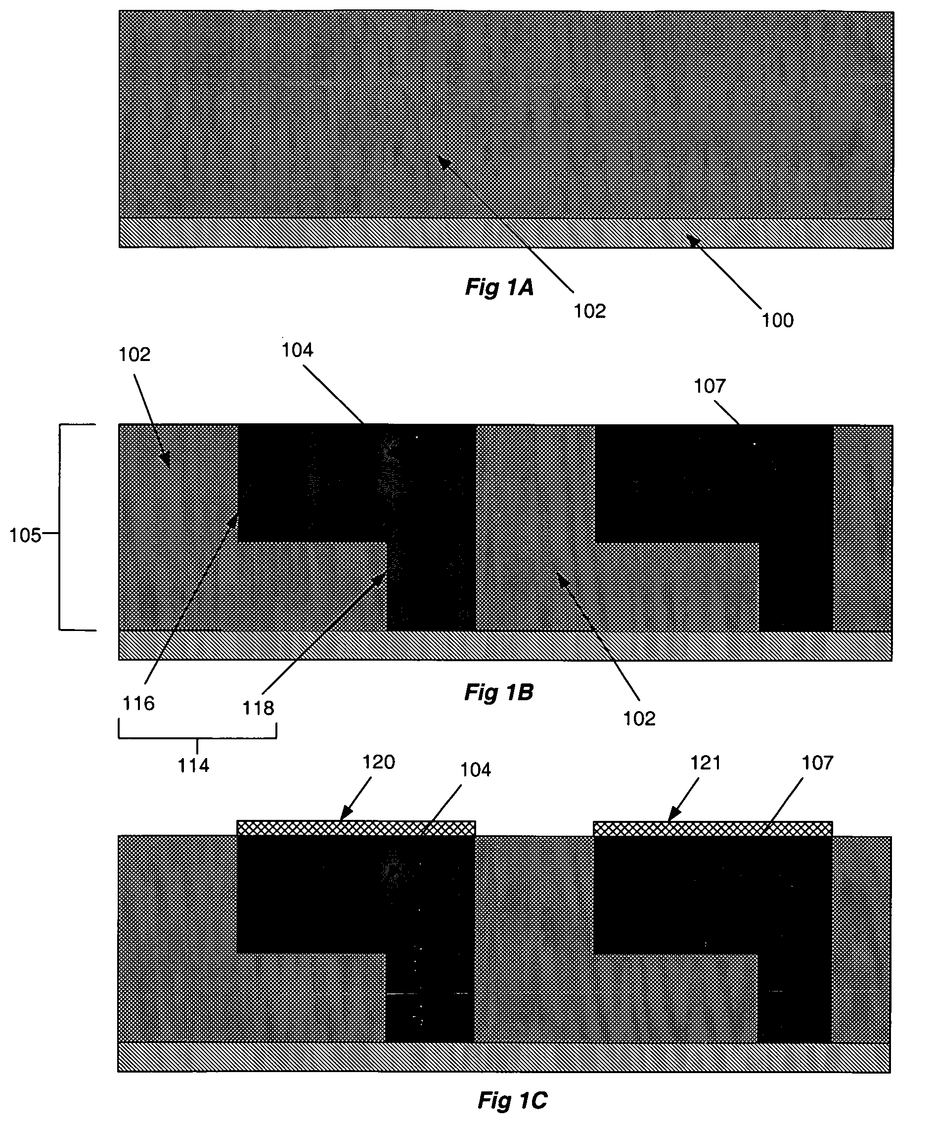
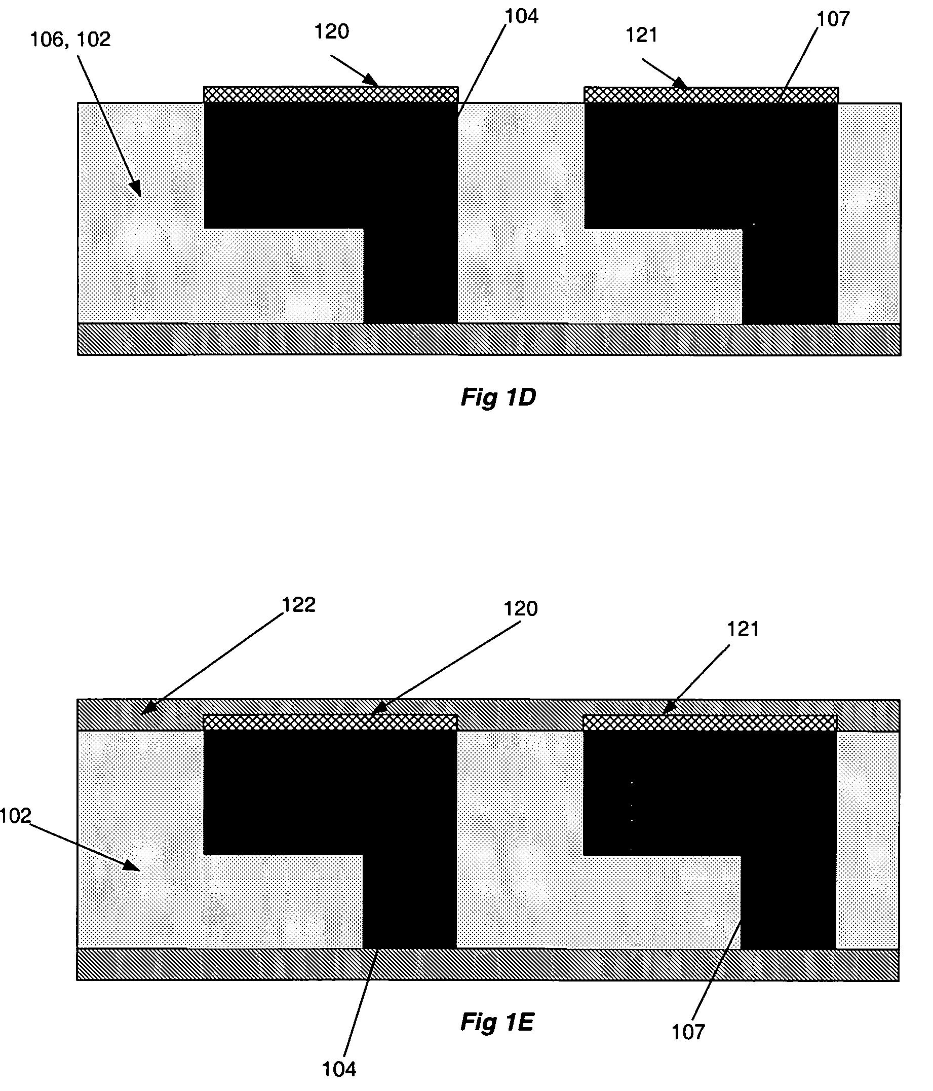
[0007]Referring to FIG. 1A, a substrate layer (100) is shown in cross section adjacent a first inter-layer dielectric (hereinafter “ILD”) layer (102). The substrate (100) may be any surface generated when making an integrated circuit, upon which a conductive layer may be formed. Substrate (100) thus may comprise, for example, active and passive devices that are formed on a silicon wafer, such as transistors, capacitors, resistors, diffused junctions, gate electrodes, local interconnects, etcetera. Substrate (100) may ...


PUM

PropertyMeasurementUnit
temperatureaaaaaaaaaa
diameteraaaaaaaaaa
diameteraaaaaaaaaa

Abstract

An inter-layer dielectric structure and method of making such structure are disclosed. A composite dielectric layer, initially comprising a porous matrix and a porogen, is formed. Subsequent to other processing treatments, the porogen is decomposed and removed from at least a portion of the porous matrix, leaving voids defined by the porous matrix in areas previously occupied by the porogen. The resultant structure has a desirably low k value as a result of the porosity and materials comprising the porous matrix and porogen. The composite dielectric layer may be used in concert with other dielectric layers of varying porosity, dimensions, and material properties to provide varied mechanical and electrical performance profiles.

Description

RELATED APPLICATIONS[0001]This application is a continuation-in-part of the patent application entitled, “Selectively Converted Inter-Layer Dielectric,” Ser. No. 10 / 302,073, which was filed on Nov. 21, 2002, now U.S. Pat. No. 6,943,121.BACKGROUND OF THE INVENTION[0002]Low dielectric constant materials are used as interlayer dielectrics in microelectronic structures, such as semiconductor structures, to reduce the RC delay and improve device performance. As device sizes continue to shrink, the dielectric constant of the material between metal lines must also decrease to maintain the improvement. Certain low-k materials have been proposed, including various carbon-containing materials such as organic polymers and carbon-doped oxides. Although such materials may serve to lower the dielectric constant, they may offer inferior mechanical properties such as poor strength and low fracture toughness. The eventual limit for a dielectric constant is k=1, which is the value for a vacuum. Metho...

Claims


Application Information

Patent Timeline
Patent Type & Authority Patents(United States)
IPC IPC(8): H01L21/302H01L21/461H01L21/469H01L21/4763H01L21/312H01L21/316H01L21/768
CPCH01L21/02118H01L21/02126H01L21/02203H01L21/02362H01L21/76835H01L21/31695H01L21/76807H01L21/7682H01L21/312H01L21/3124H01L2221/1036H01L2221/1047
Inventor KLOSTER, GRANT M.O'BRIEN, KEVIN P.GOODNER, MICHAEL D.LEU, JIHPERNGGRACIAS, DAVID H.ROCKFORD, LEE D.MOON, PETER K.BARNS, CHRIS E.
Owner INTEL CORP
Why Eureka
Try Eureka