Radiation detector, scintillator panel, and methods for manufacturing same

a technology of scintillator and detector, which is applied in the direction of radiation intensity measurement, x/gamma/cosmic radiation measurement, instruments, etc., can solve the problems of reducing the resolution in the vicinity of the joint, affecting the detection accuracy of scintillators, so as to achieve the effect of preventing the scintillator from peeling off, reducing the width of the area at the joint, and reducing the sensibil sensibility

Inactive Publication Date: 2006-03-28
HAMAMATSU PHOTONICS KK
View PDF19 Cites 10 Cited by
  • Summary
  • Abstract
  • Description
  • Claims
  • Application Information

AI Technical Summary

Benefits of technology

[0009]In the image sensor panels or scintillator-forming substrates obtained in this way, when the sidewalls where the scintillators are formed are disposed so as to adjacent these sidewalls and fixed to each other, a large-screen radiation detector or a scintillator panel for a large screen can be obtained. According to the present invention, an almost uniform scintillator extending to an edge is formed, and therefore the width of an area low in sensibility that arises at a joint can be controlled to a minimum.
[0010]Preferably, the image sensor panel has at least one of a circuit section electrically connected to the photoelectric detectors and a bonding pad between at least one of the other sides that are not adjacent to the light receiving section of the image sensor panel and the light receiving section thereof. Thereby, the readout line of an electrical signal can be easily formed.
[0011]Preferably, a moisture-proof protective film covering the scintillator is provided. Thereby, the scintillator can be further effectively prevented from peeling off.

Problems solved by technology

However, there is a problem that a scintillator is liable to separate from a boundary (a joint) with an adjoining detector when a plurality of detectors are arranged to make a large screen in this way.
This problem causes a concern that the resolution in the vicinity of the joint will decrease or that the scintillator will completely separate therefrom.

Method used


Image

  • Radiation detector, scintillator panel, and methods for manufacturing same
  • Radiation detector, scintillator panel, and methods for manufacturing same
  • Radiation detector, scintillator panel, and methods for manufacturing same

Examples


second embodiment

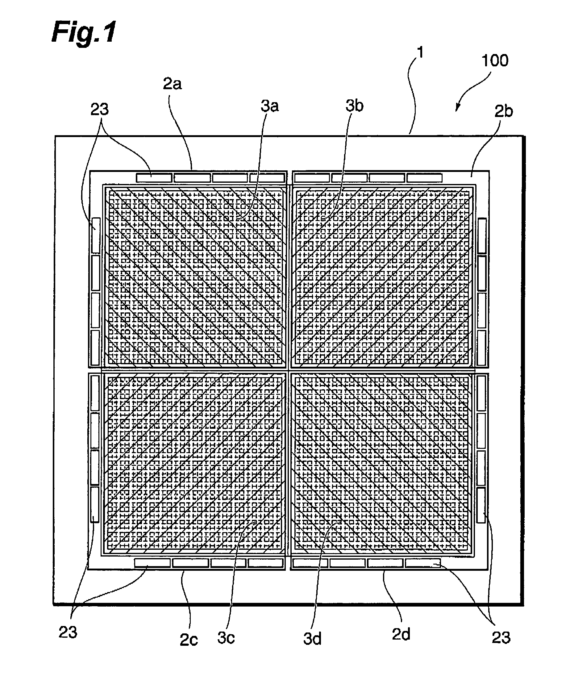
[0037]FIG. 13 is a plan view showing the radiation detector according to the present invention. As shown in this figure, the solid-state image sensing devices 2a and 2b that are two image sensor panels may be coupled together to manufacture a radiation detector with a large screen. Further, it is allowable to arrange three or more solid-state image sensing devices in a row so as to make a large screen or arrange them in 2×m array or in m×n array for a large screen. If the solid-state image sensing devices are arranged in 2×m array (where m is 3 or an integer greater than 3), solid-state image sensing devices 2′ other than the image sensing device disposed at at least four corners are required to have a structure (see FIG. 14) in which the light receiving section 22 is disposed up to the boundary of at least three sides. If the solid-state image sensing devices are arranged in m×n array (where m and n are each 3 or an integer greater than 3), solid-state image sensing devices 2″ disp...

third embodiment

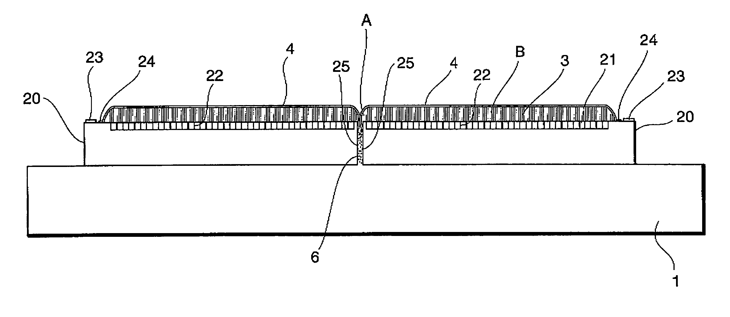
[0038]FIG. 16 is a sectional view showing the radiation detector according to the present invention. Scintillator panels 6a and 6b according to the present invention are disposed on the solid-state image sensing devices 2. In each scintillator panel 6, the scintillator 3 successively extends from one side face 61 of a glass board 60, which serves as a scintillator-forming substrate, toward the sidewall 62, and a protective film 4 of Parylene is formed so as to cover and wrap the scintillator 3. The scintillator panels 6a and 6b are disposed on the light receiving section 22 of one solid-state image sensing device 2 in a state where the sidewalls 62 butt against each other, and a side where the scintillator 3 is formed is directed to the solid-state image sensing device 2.

first embodiment

[0039]Since a method for manufacturing the scintillator panel 6 follows the steps shown in FIG. 4 to FIG. 8, a description thereof is omitted. When this scintillator panel 6 is used, the same effect as the radiation detector of the first embodiment can be obtained. Not only on the side of the scintillator panel 6 but also on the side of the solid-state image sensing device 2, a plurality of solid-state image sensing devices may be combined like a panel. If the scintillator side of the scintillator panel is directed to the light receiving section of the solid-state image sensing device, the board 60 forming the scintillator needs to be radiolucent. Al- or Be made board, instead of glass, or a material mainly composed of carbon, such as amorphous carbon or graphite, can be used as a radiolucent board.

[0040]If the side of the board 60 of the scintillator panel is directed to the light receiving section of the solid-state image sensing device, the board needs to be transmissible to ligh...


PUM


Abstract

An image sensor panel (2) has a light receiving section (22) consisting of a plurality of photoelectric detectors (21) two-dimensionally arranged close to corners on a substrate (20). The image sensor panel (2) has a scintillator (3) formed successively from the surface of the light receiving section (22) to sidewall parts (25) close thereto. A screen is enlarged by butting the sidewall parts (25) against each other.

Description

TECHNICAL FIELD[0001]This invention relates to a radiation detector and a scintillator panel, and, more particularly, to a radiation detector and a scintillator panel that can be suitably applied to a radiation imaging device constructed by arranging a plurality of image sensors so as to pick up a radiation image having a large image area, and to methods for manufacturing them.BACKGROUND ART[0002]An X-ray image sensor using a CCD, in place of an X-ray photosensitive film, has been widely employed as an X-ray diagnostic instrument for medical use. In such a radiation imaging system, two-dimensional image data by radiation is obtained as an electrical signal by use of a radiation detector that has a plurality of pixels, and an X-ray image is displayed on a monitor by processing the signal with a processor. A typical radiation detector has a mechanism in which a scintillator is disposed on photodetectors arranged one-dimensionally or two-dimensionally, and incident radiations are trans...

Claims


Application Information

Patent Timeline
Patent Type & Authority Patents(United States)
IPC IPC(8): G01T1/24G01T1/20G01T1/29H01L31/09
CPCG01T1/2018G01T1/20189
Inventor TAKABAYASHI, TOSHIOHOMME, TAKUYA
Owner HAMAMATSU PHOTONICS KK
Why Eureka
Try Eureka