This helps you quickly interpret patents by identifying the three key elements:
Problems solved by technology
Method used
Benefits of technology
Benefits of technology
[0008]In the above QFN manufacturing process, a semiconductor chip is mounted on a die pad portion of a lead frame, the semiconductor chip and leads are connected with each other using wires, then the lead frame is loaded into a molding die to seal the semiconductor chip with resin, and thereafter unnecessary portions of the lead frame exposed to the exterior of the resin sealing member are cut off with a dicer. At this time, metallic burrs occur in the cut faces of the leads, causing a lowering in the production yield of QFN. If the lead frame dicing speed with the dicer is set low, the occurrence of metallic burrs will be decreased, but the productivity of QFN is deteriorated because the lead frame dicing work consumes much time.
[0009]Further, in the lead frame referred to above, lead patterns are formed by etching or pressing a metallic sheet, so if an attempt is made to attain a multi-pin structure of QFN and narrow the lead pitch, it is necessary to thin the metallic sheet used in fabricating the lead frame. As a result, leads and suspension leads become less rigid and a positional deviation of the semiconductor chip becomes easy to occur due to flowing of molten resin at the time of sealing the semiconductor chip with resin.
[0010]It is an object of the present invention to provide a technique for improving the production yield of QFN.
[0011]It is another object of the present invention to provide a technique capable of promoting a multi-pin structure of QFN.
Problems solved by technology
At this time, metallic burrs occur in the cut faces of the leads, causing a lowering in the production yield of QFN.
If the lead frame dicing speed with the dicer is set low, the occurrence of metallic burrs will be decreased, but the productivity of QFN is deteriorated because the lead frame dicing work consumes much time.
Method used
Image
Click on the blue label to locate the original text in one second.
Reading with bidirectional positioning of images and text.
Examples
first embodiment
(First Embodiment)
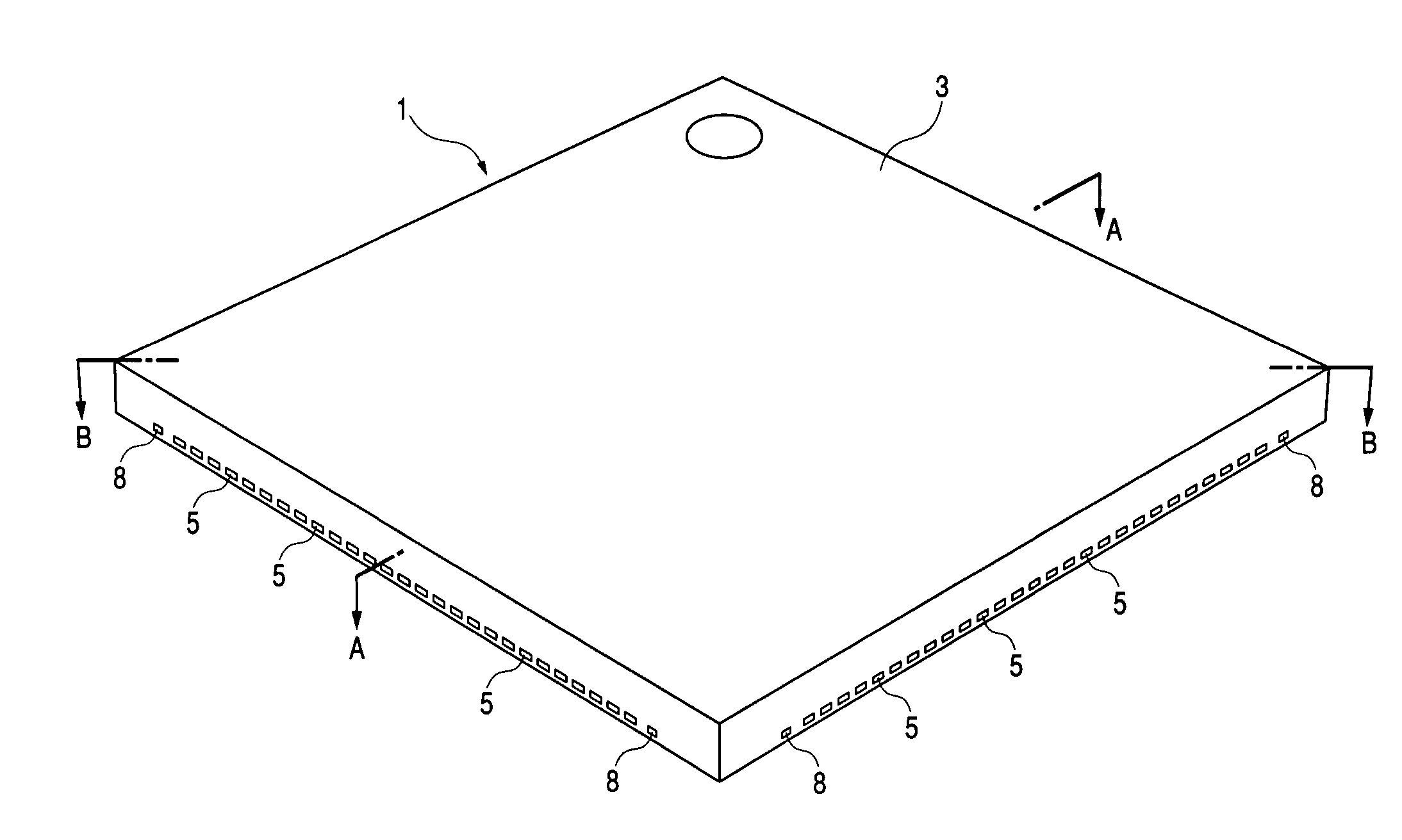
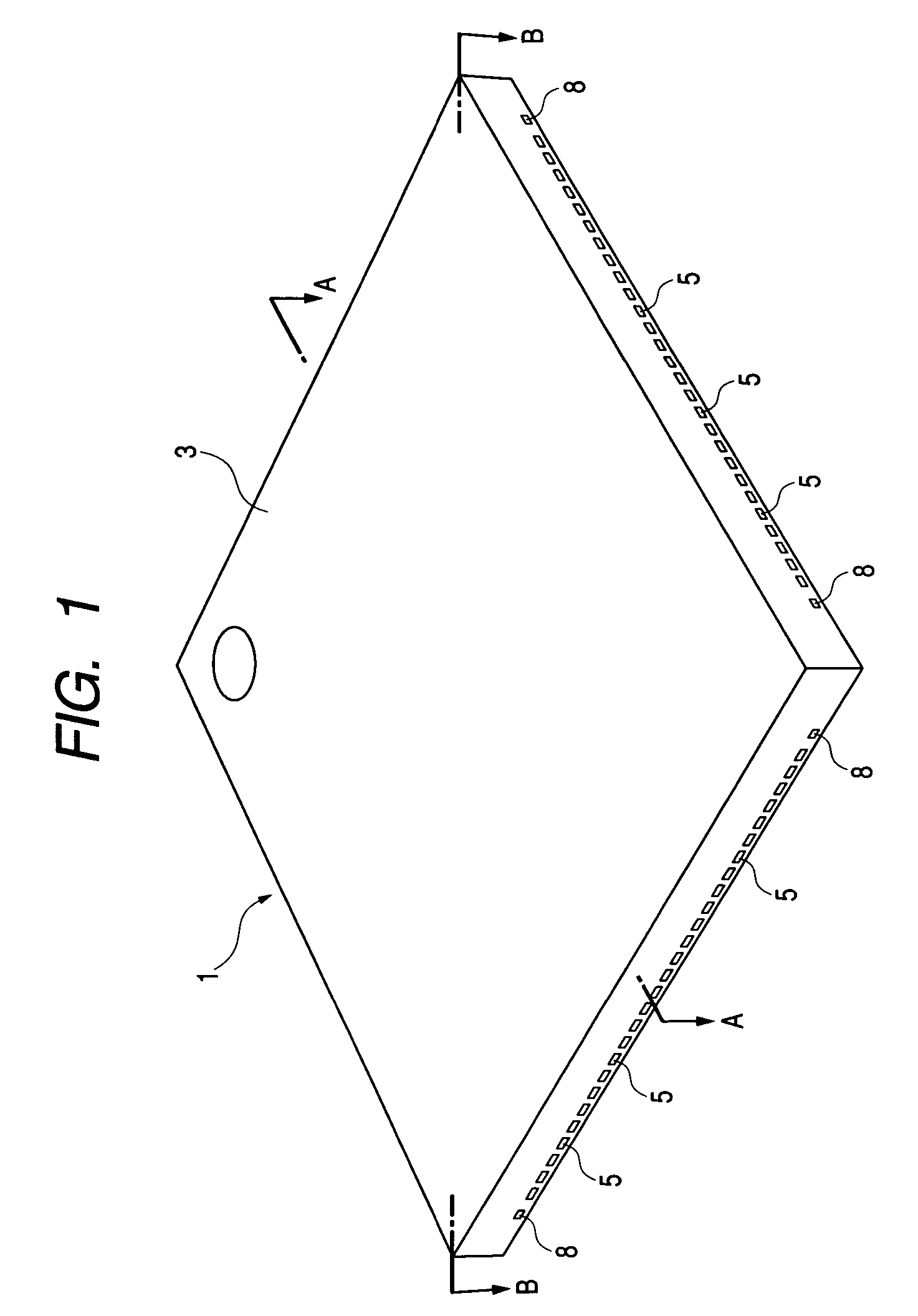
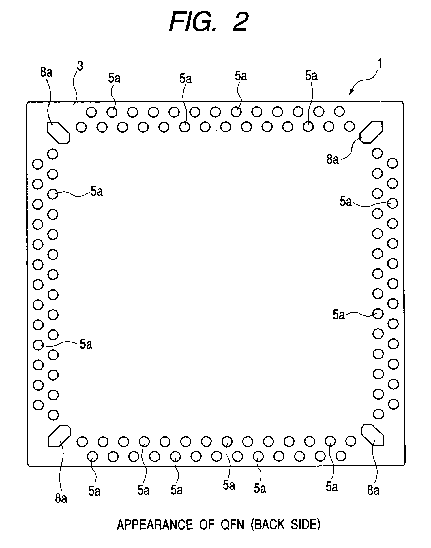
[0080]FIG. 1 is a perspective view showing an appearance of a QFN according to an embodiment of the present invention, FIG. 2 is a plan view showing an appearance (back surface) of the QFN, FIG. 3 is a plan view showing an internal structure (surface side) of the QFN, FIG. 4 is a plan view showing an internal structure (back surface) of the QFN, FIG. 5 is a side view of the QFN, FIG. 6 is a sectional view taken along line A—A in FIG. 1, and FIG. 7 is a sectional view taken along line B—B in FIG. 1.
[0081]The QFN of this embodiment, indicated at 1, is a surface-mounted type package wherein one semiconductor chip 2 is sealed with a resin sealing member 3. It external dimensions are, for example, 12 mm long, 12 mm wide, and 1.0 mm thick.
[0082]A semiconductor chip 2 is mounted on an upper surface of a metallic die pad portion 4 and in this state is disposed at a center of a resin sealing member 3. The die pad portion 4 is formed as a so-called small tab structure wherei...
second embodiment
(Second Embodiment)
[0116]FIG. 35 is a plan view showing a part of the lead frame LF2 used in manufacturing the QFN 1, FIG. 36 is a sectional view taken along line Y–Y′ in FIG. 35, and FIG. 37 is a sectional view taken along line Z–Z′ in FIG. 35.
[0117]As shown in the figures, each of plural leads 5 formed in a lead frame LF2 used in this embodiment is different in thickness between inside (closer to a die pad portion 4) and outside of the portion where each of terminals 5a is formed. More specifically, in each lead 5, the thickness (t′) of an outside portion (FIG. 36) of the terminal 5a is larger than the thickness (t) of an inside portion (FIG. 37) of the terminal 5a (t′>t).
[0118]The lead frame LF2 is fabricated by the method of half-etching a metallic sheet 10 described in the previous first embodiment (see FIGS. 9 and 10), but a difference from the first embodiment resides in that, at the time of forming photoresist films 11 on one side of the lead-forming area of the metallic she...
third embodiment
(Third Embodiment)
[0123]FIG. 44 is a plan view showing a part of a surface of a lead frame LF3 used in manufacturing QF1, FIG. 45 is a plan view showing a part of a back surface of the lead frame LF3, and FIG. 45 is a perspective view showing a central portion (the area where a die pad portion 4 is formed) on a larger scale.
[0124]The lead frame LF3 is characteristic in that plural projections 4a are formed along an outer periphery of a back surface of the die pad portion 4. As shown in FIG. 47, the projections 4a are formed simultaneously with forming patterns (die pad portion 4, leads 5, suspension leads 8) of the lead frame LF3. More specifically, there is provided a metallic sheet 10 of, for example, Cu, Cu alloy, or Fe—Ni alloy having a thickness of 125 to 150 μm, and one side of the metallic sheet 10 is coated with photoresist film 11 in portions where a die pad 4 and leads 5 (and suspension leads 8 not shown) are to be formed. In portions where terminals 5a and projections 4a ...
PUM
Abstract
It is intended to improve the production yield of QFN (Quad Flat Non-leaded package) and attain a multi-pin structure. After a resin sealing member for sealing a semiconductorchip is formed by molding, a peripheral portion of the resin sealing member and a lead frame are both cut along a cutting line which is positioned inside (on a central side of the resin sealing member) of a line (molding line) extending along an outer edge of the resin sealing member, whereby the whole surface (upper and lower surfaces and both side faces) of each of leads exposed to side faces (cut faces) of the resin sealing member is covered with resin, thus preventing the occurrence of metallic burrs on the cut faces of the leads.
Description
BACKGROUND OF THE INVENTION[0001]The present invention relates to a semiconductor device and a method of manufacturing the same. Particularly, the present invention is concerned with a technique which is effectively applicable to a resin-sealed type semiconductor device.[0002]As a resin package wherein a semiconductor chip mounted on a lead frame is sealed with a sealing member of a molded resin there is known a QFN (Quad Flat Non-leaded package) (see, for example, Patent Literatures 1 and 2).[0003]The QFN is of a structure wherein one ends of plural leads which are electrically connected to a semiconductor chip through bonding wires are exposed from a back surface (underside) of an outer peripheral portion of a sealing member to constitute terminals, and bonding wires are connected to the surfaces opposite to the exposed surfaces of the terminals, i.e., to terminal surfaces in the interior of the sealing member, to connect the terminals and the semiconductor chip electrically with ...
Claims
Application Information
Patent Timeline
Application Date:The date an application was filed.
Publication Date:The date a patent or application was officially published.
First Publication Date:The earliest publication date of a patent with the same application number.
Issue Date:Publication date of the patent grant document.
PCT Entry Date:The Entry date of PCT National Phase.
Estimated Expiry Date:The statutory expiry date of a patent right according to the Patent Law, and it is the longest term of protection that the patent right can achieve without the termination of the patent right due to other reasons(Term extension factor has been taken into account ).
Invalid Date:Actual expiry date is based on effective date or publication date of legal transaction data of invalid patent.

