High frequency module and antenna device

a high frequency module and antenna technology, applied in the direction of antennas, electrical equipment, transmission, etc., can solve the problems of limiting the flexibility of a configuration of a constituent circuit, affecting the operation of the antenna device, so as to improve the flexibility of a configuration of the constituent circui

Inactive Publication Date: 2006-03-28
MITSUBISHI ELECTRIC CORP
View PDF9 Cites 14 Cited by
  • Summary
  • Abstract
  • Description
  • Claims
  • Application Information

AI Technical Summary

Benefits of technology

[0012]The present invention has been made in order to solve the problems mentioned above. An object of the invention is to obtain a high frequency module which enables an antenna apparatus to be made compact and lightweight and enhances flexibility of a configuration of constituent circuits, and a compact and lightweight antenna apparatus.

Problems solved by technology

This has resulted in a problem in that the primary radiator 61, the polarizer 62, the orthomode transducer 63, the diplexers 64a and 64b and the receiver must be located in proximity, which restricts flexibility of a configuration of those circuits.
This has resulted in a problem in that a machine-driven part of the antenna apparatus grows large and heavy, and its rotating mechanism and rotation supporting mechanism grow large and heavy.

Method used


Image

  • High frequency module and antenna device
  • High frequency module and antenna device
  • High frequency module and antenna device

Examples


embodiment 1

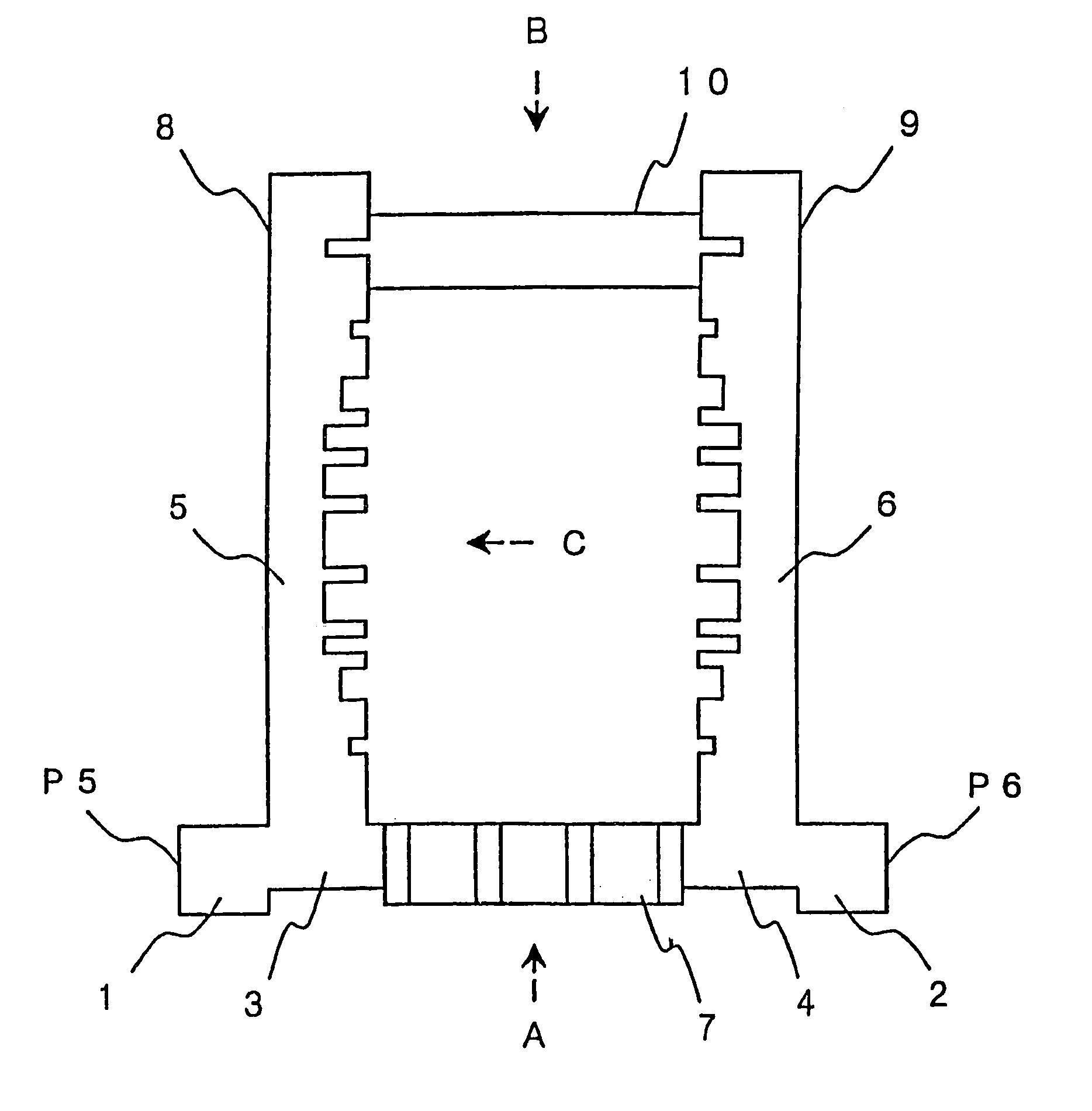
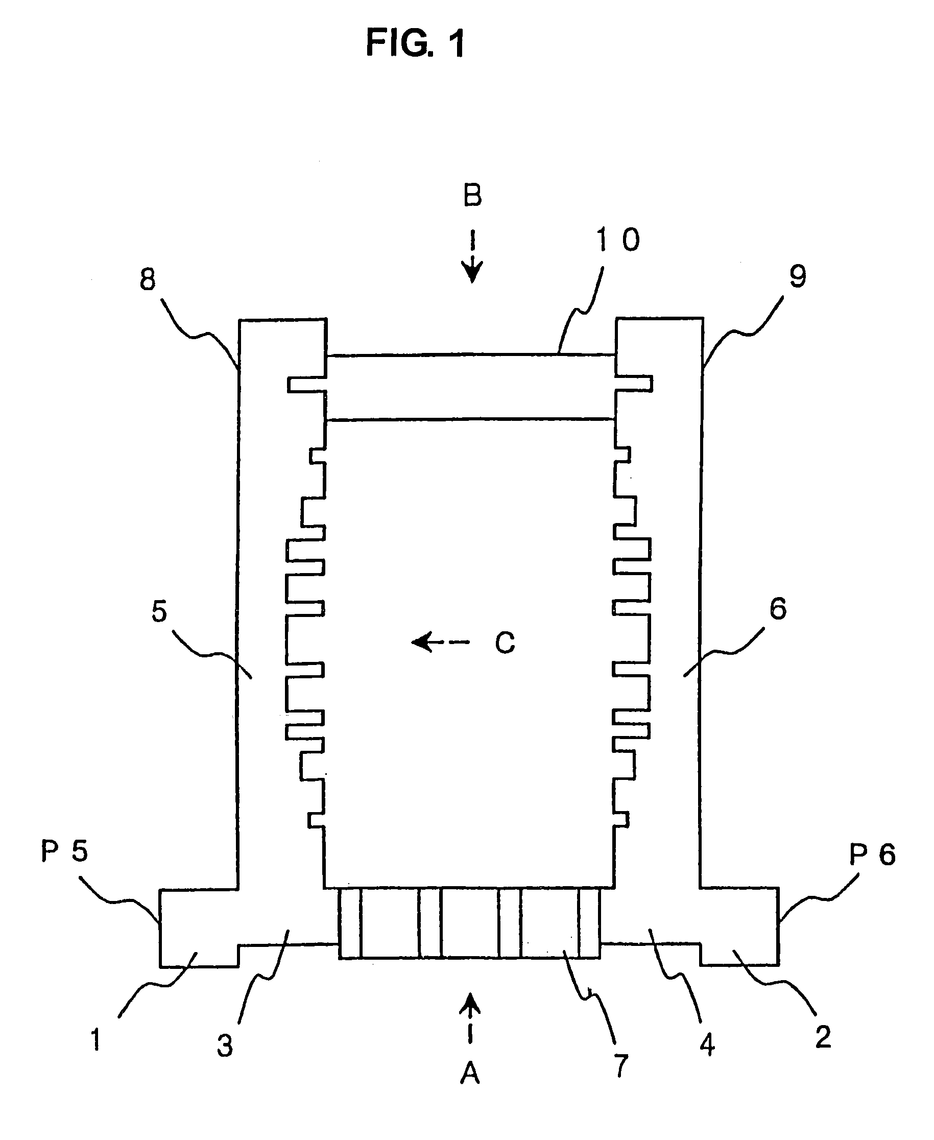
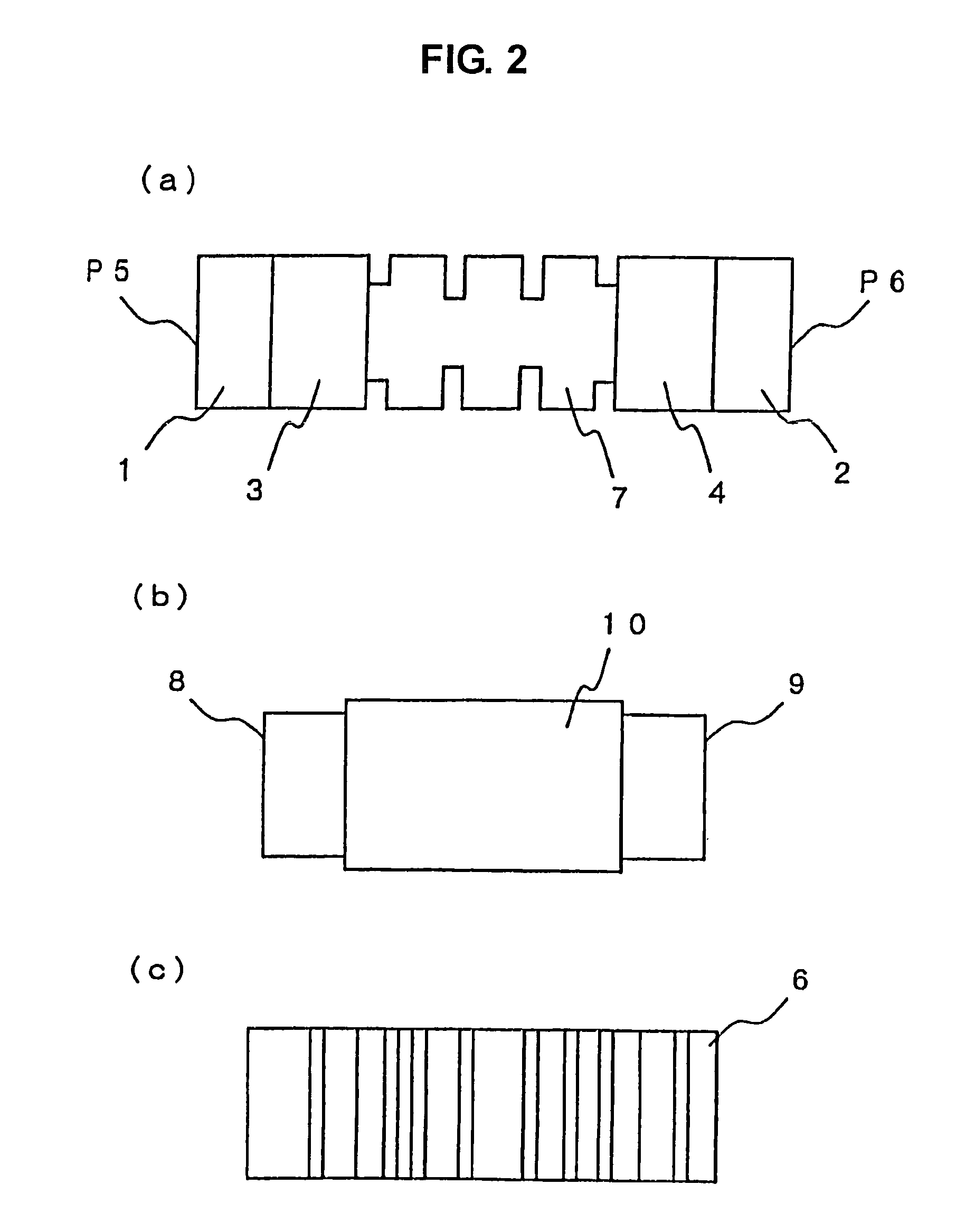
[0045]FIG. 1 is a top view showing an arrangement of a high frequency module in Embodiment 1 of the present invention, FIG. 2(a) is a side elevation viewed from a direction A of FIG. 1, FIG. 2(b) is a side elevation of a low noise amplifier viewed from a direction B of FIG. 1, and FIG. 2(c) is an internal side elevation viewed from a direction C of FIG. 1. In those figures, reference numeral 1 denotes a rectangular main waveguide (first main waveguide) in which high frequency radio waves are inputted / outputted from an input / output terminal P5 to be described below; 2, a rectangular main waveguide (second main waveguide) in which high frequency radio waves are inputted / outputted from an input / output terminal P6 to be described below; 3, an E-plane T-branch circuit (first T-branch circuit) of a stepped rectangular waveguide in which the E-planes of the rectangular waveguide each have a T-shape and its branch portion (branch point) is provided with a matching step; 4, an E-plane T-bran...

embodiment 2

[0056]FIG. 3 is a top view showing an arrangement of a high frequency module according to Embodiment 2 of the present invention, FIG. 4(a) is a side elevation viewed from a direction A of FIG. 3, FIG. 4(b) is a side elevation of a low noise amplifier viewed from a direction B of FIG. 3, and FIG. 4(c) is an internal side elevation viewed from a direction C of FIG. 3.

[0057]In Embodiment 1 described above, the band-pass filter 7 is illustratively connected to the rectangular waveguide E-plane T-branch circuits 3 and 4. As shown in FIG. 3, however, the band-pass filter 7 is replaced by an inductive iris-coupled rectangular waveguide band-pass filter 11 (first band-pass filter) which is connected to the E-plane T-branch circuit 3 and which has a partially bent longitudinal axis, a rectangular waveguide E-plane bend 13 (first bend) connected to the band-pass filter 11, a rectangular waveguide E-plane bend 14 (second bend) connected to the rectangular waveguide E-plane bend 13, and an indu...

embodiment 3

[0061]FIG. 5 is a top view showing an arrangement of a high frequency module according to Embodiment 3 of the present invention, FIG. 6(a) is a side elevation viewed from a direction A of FIG. 1, FIG. 6(b) is a side elevation of a low noise amplifier viewed from a direction B of FIG. 5, and FIG. 6(c) is a side elevation viewed from a direction C of FIG. 5. In Embodiment 1 described above, the low-pass filters 5 and 6 are illustratively connected to the rectangular waveguide E-plane T-branch circuits 3 and 4. As shown in FIG. 5, however, the low-pass filters 5 and 6 are replaced by inductive iris-coupled rectangular waveguide band-pass filters 15 and 16 (first band-pass filter and third band-pass filter). Note that the band-pass filter 7 corresponds to the second band-pass filter.

[0062]Here, the inductive iris-coupled rectangular waveguide band-pass filters 15 and 16 used in Embodiment 3 each have a structure similar to that of the inductive iris-coupled rectangular waveguide band-pa...


PUM


Abstract

The present invention includes: a first main waveguide 1; a T-branch circuit 3 connected thereto; a first low-pass filter 5 connected thereto; a band-pass filter 7 connected to the first T-branch circuit 3; a first converter 8 connected to the first low-pass filter 5 for converting transmission lines between a waveguide and a microwave integrated circuit; an amplifier 10 connected to the first converter and structured by the microwave integrated circuit; a second converter 9 connected thereto for converting transmission lines between a waveguide and the microwave integrated circuit; a second low-pass filter 6 connected thereto; a second T-branch circuit 4 connected to the second low-pass filter and the band-pass filter 7; and a second main waveguide 2 connected to the second T-branch circuit.

Description

[0001]This application is a 371 of PCT / JP03 / 03451 filed Mar. 3, 2003.TECHNICAL FIELD[0002]The present invention relates to a high frequency module that is used mainly in VHF, UHF, microwave and millimeter wave bands, and more particularly to an antenna apparatus using the same.BACKGROUND ART[0003]FIG. 19 shows an arrangement of an antenna apparatus for shared use of left / right-handed circularly polarized waves and two frequency bands set forth, for example, in Takashi Kitsuregawa, “Advanced Technology in Satellite Communication Antennas: Electrical & Mechanical Design”, ARTECH HOUSE INC., pp. 193–195, 1990.[0004]In the figure, reference numeral 61 denotes a primary radiator for transmitting both left- and right-handed circularly polarized waves in a first frequency band to a main- or sub-reflector and for receiving both left- and right-handed circularly polarized waves in a second frequency band from the main- or sub-reflector; 62, a polarizer; 63, an orthomode transducer; 64a and 6...

Claims


Application Information

Patent Timeline
Patent Type & Authority Patents(United States)
IPC IPC(8): H01Q13/00H01P1/208H01P1/211H01P1/213H04B1/40
CPCH01P1/2138H01P1/2131
Inventor YONEDA, NAOFUMIMIYAZAKI, MORIYASUOHWADA, TETSUOH-HASHI, HIDEYUKIYAMANAKA, KOJIMORI, KAZUTOMIIKEDA, YUKIOHORIE, TOSHIYUKIIIDA, AKIOOZAKI, YUTAKA
Owner MITSUBISHI ELECTRIC CORP
Why Eureka
Try Eureka