Semiconductor memory apparatus and self-repair method

a memory apparatus and semiconductor technology, applied in the direction of digital storage, electronic circuit testing, instruments, etc., can solve the problems of almost impossible to increase the yield to 100%, the apparatus cannot of course be shipped as a product, and the yield becomes a big problem of fabrication

Inactive Publication Date: 2006-03-28
SONY CORP
View PDF5 Cites 13 Cited by
  • Summary
  • Abstract
  • Description
  • Claims
  • Application Information

AI Technical Summary

Benefits of technology

[0015]It is thus an object of the present invention addressing the problems described above to provide a semiconductor memory apparatus capable of carrying out a repair search at a high speed but at a small circuit scale in a configuration providing a BIST circuit embedded in the semiconductor memory apparatus with a repair-search function and provide a self-repair method capable of carrying out a self repair completely on the chip of the semiconductor memory apparatus.
[0042]As described above, in accordance with the present invention, redundant lines are used in a structure where the redundant lines are shared by a plurality of redundant blocks laid out in two-dimensional directions. In this case, the mask address of a redundant line can be determined in an on-chip process. With such an on-chip process, an abnormal bit can be repaired not only at the time the chip is shipped from the factory, but also after the chip is delivered to the user as a product by carrying out the BISR function typically at the time the power supply is turned on. Thus, the present invention exhibits an effect to increase the probability of rescuing the chip from abnormal bits.
[0043]In addition, by storing information obtained as a result of evaluation of individual memory cells to determine whether the memory cells are good or defective in a buffer as a smallest amount of address information required for determining redundant lines each to serve as a substitute for an abnormal memory cell, the BISR function can be implemented by using a small size of the buffer and a small circuit scale in comparison with a case in which all address information obtained as the evaluation result is stored in a buffer. In addition, since a repair search is carried out in the same chip as the memory unit, the repair search can be carried out at a high processing speed.

Problems solved by technology

In a semiconductor memory apparatus such as a DRAM, the integration scale is extremely large and, in consequence, the yield becomes a big problem of fabrication in recent years.
Practically, it is almost impossible to increase the yield to 100% so that one may assume that a defective memory cell always exists in a semiconductor memory apparatus.
If a defective memory cell exists in a semiconductor memory apparatus, however, the apparatus cannot of course be shipped as a product.
It is thus practically difficult to test the individual memories of the same LSI chip independently of each other.
In addition, as the operating speed of the LSI chip becomes higher, it becomes difficult to evaluate the performance of a memory by using an external memory tester.
In addition, even if a memory can be tested by using an external memory tester, such a memory tester is extremely expensive.
Even in the case of an LSI chip including an embedded BIST circuit, however, a problem remains to be solved if the chip is tested in a configuration wherein information on normality / abnormality for each bit is transferred to a memory of an external computer and the external computer is used for carrying out a repair-search calculation as is the case with the conventional technology disclosed in patent reference 1.
This is because a memory with a large storage capacity for storing the information on normality / abnormality for each bit is required of the external computer and it takes very long time to carry out the calculation.

Method used


Image

  • Semiconductor memory apparatus and self-repair method
  • Semiconductor memory apparatus and self-repair method
  • Semiconductor memory apparatus and self-repair method

Examples


Embodiment Construction

[0055]Preferred embodiments of the present invention are described in detail by referring to the diagrams as follows.

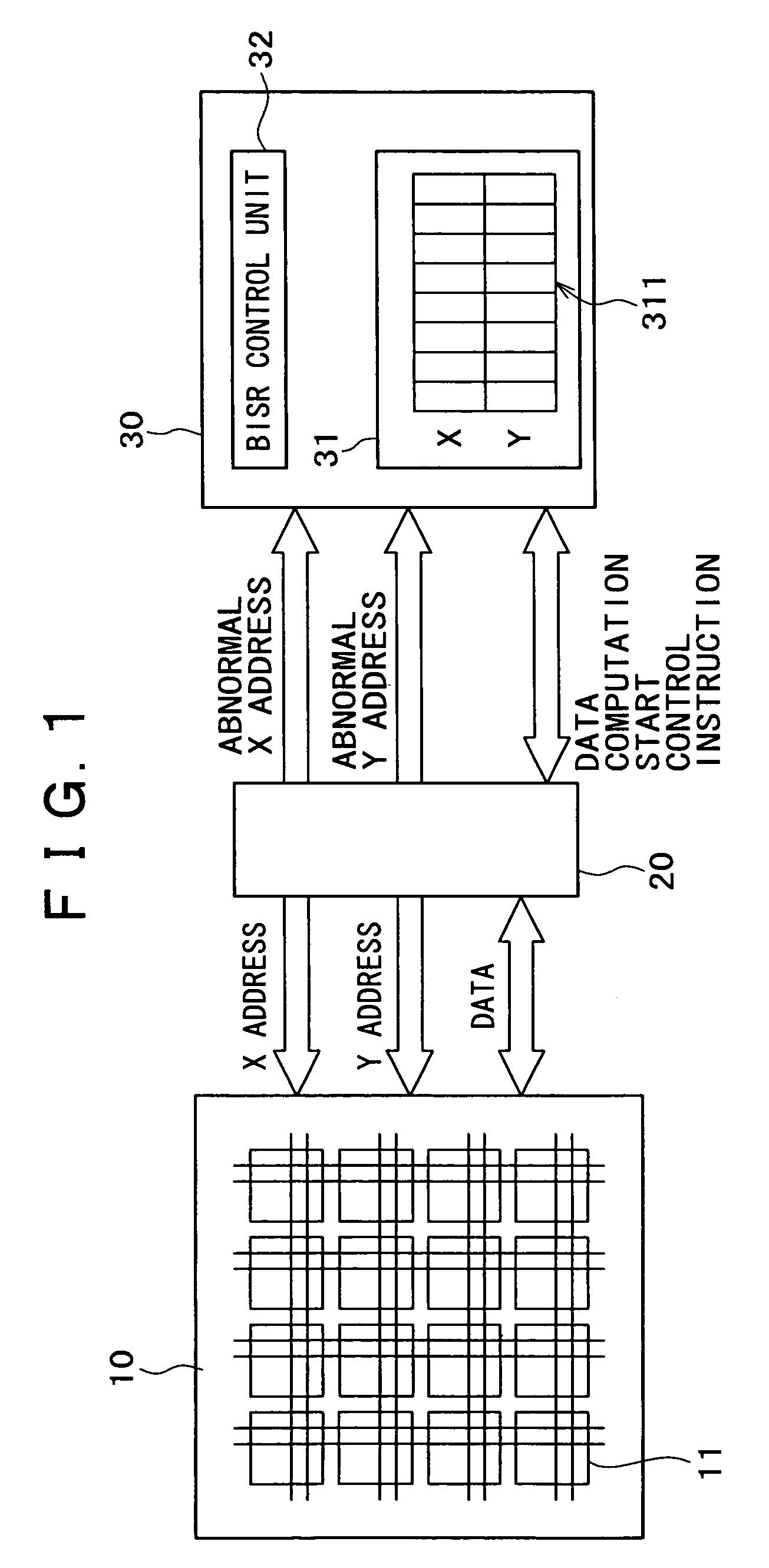
[0056]FIG. 1 is a block diagram showing a typical configuration of a semiconductor memory apparatus implemented by an embodiment of the present invention. As is obvious from FIG. 1, the semiconductor memory apparatus implemented by the embodiment as an LSI chip includes a RAM (or memory unit) 10 such as a DRAM or an SRAM, a BIST (Built-In Self-Test) circuit 20 and a BISR (Built-In Self-Repair) circuit 30. The RAM 10, the BIST circuit 20 and the BISR circuit 30 are included in the same LSI chip.

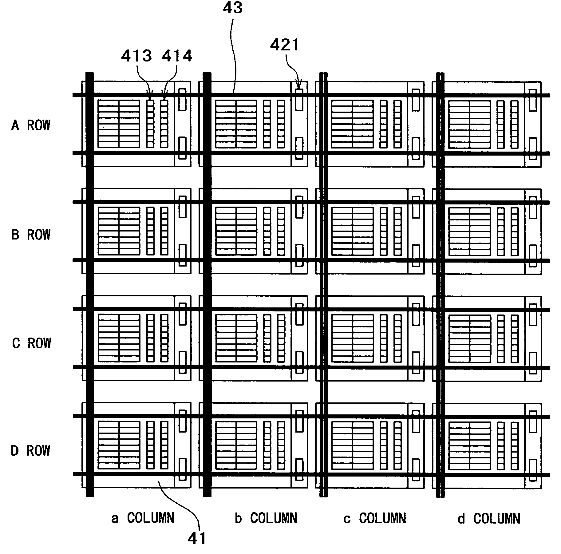
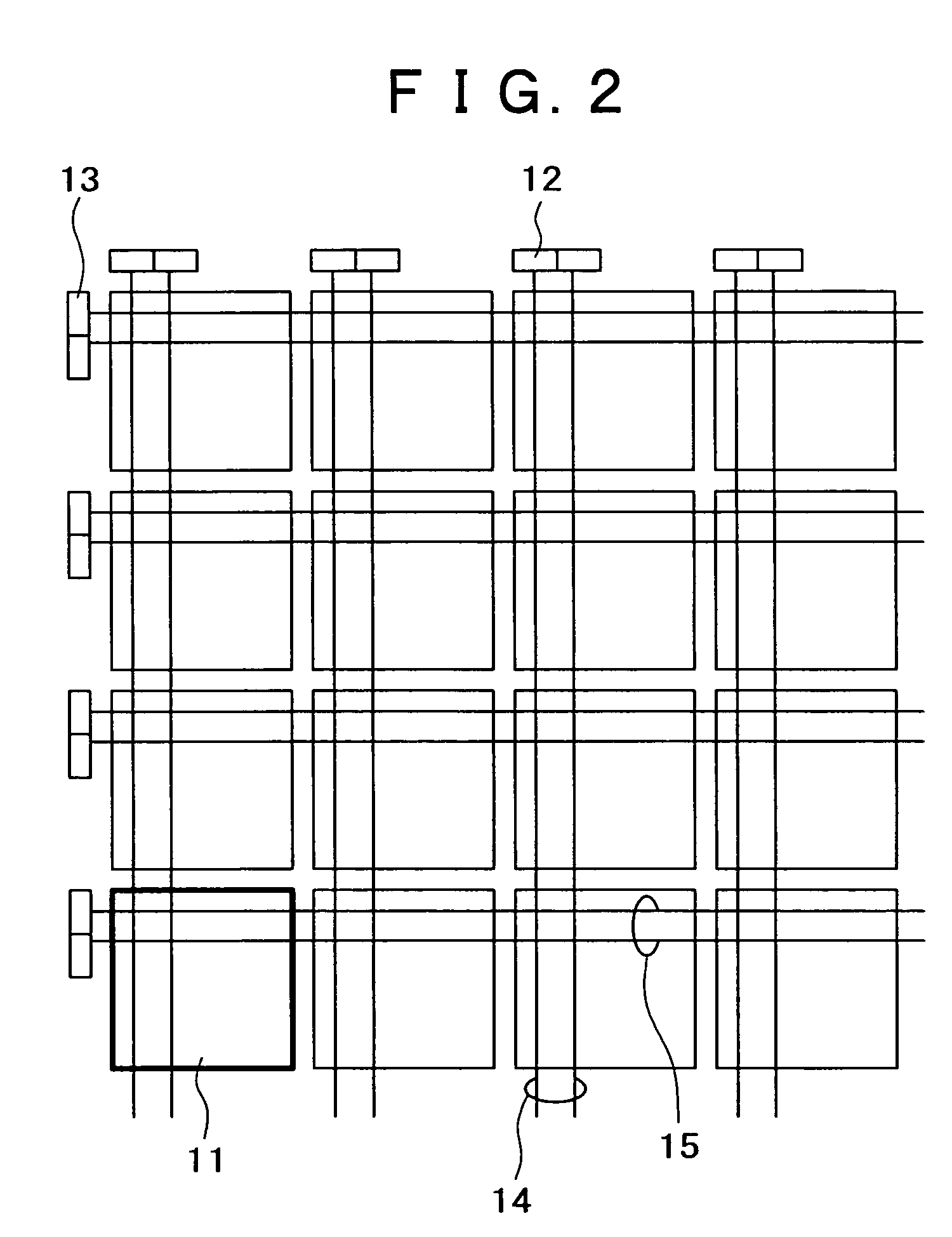
[0057]As shown in FIG. 2, the RAM 10 generally includes small unit blocks 11 having a memory core, which includes a plurality of memory cells laid out to form a matrix, and spare memory cells each serving as a redundant memory cell used for repairing an abnormal memory cell generated in a memory core. The small unit blocks 11 are each referred to hereafter as a redundant block 1...


PUM


Abstract

A memory unit includes unit blocks laid out to form a block matrix. Each of the unit blocks has a plurality of memory cells laid out to form a cell matrix and redundant lines including redundant memory cells each used for repairing an abnormal memory cell. Every plurality of unit blocks forms a two-dimensional group oriented in a first direction and a second direction, and the redundant lines connected in the first and second directions are shared by the unit blocks pertaining to the two-dimensional group. Self-repair means embedded in the same chip as the memory unit stores only a minimum number of address pairs in storage means provided for each of the unit blocks as address pairs required for determining a redundant line to be used for repairing an abnormal memory cell and, then, finds a redundant line to be used for repairing an abnormal memory cell for each of the unit blocks pertaining to the two-dimensional group on the basis of the address pairs stored in the storage means.

Description

BACKGROUND OF THE INVENTION[0001]The present invention relates to a semiconductor memory apparatus such as a DRAM (Dynamic Random Access Memory) or an SRAM (Static Random Access Memory) as well as relates to a self-repair method adopted in the semiconductor memory apparatus. More particularly, the present invention relates to a semiconductor memory apparatus having a redundancy search circuit for replacing a bad (defective) memory cell with a redundant memory cell included in the semiconductor memory apparatus in advance as well as relates to a self-repair method adopted in the semiconductor memory apparatus.[0002]In a semiconductor memory apparatus such as a DRAM, the integration scale is extremely large and, in consequence, the yield becomes a big problem of fabrication in recent years. Practically, it is almost impossible to increase the yield to 100% so that one may assume that a defective memory cell always exists in a semiconductor memory apparatus. A defective memory cell is ...

Claims


Application Information

Patent Timeline
Patent Type & Authority Patents(United States)
IPC IPC(8): G11C7/00G11C29/00G01R31/28G11C29/04G11C29/12G11C29/44
CPCG11C29/44G11C29/4401G11C29/808G11C29/72G11C2029/1208
Inventor NAGATA, KOUKODAMA, HIROAKI
Owner SONY CORP
Why Eureka
Try Eureka