Structure of connector for reducing electro-magnetic wave interference

a technology of electro-magnetic wave interference and connector structure, which is applied in the direction of coupling device connection, two-part coupling device, electrical apparatus, etc., can solve the problems of insufficient space for circuits and electronic elements, easy generation of high-frequency electro-magnetic wave that interferes with other electronic appliances, and interference of signal from the rj45 by external transmission wires, etc., to achieve the effect of reducing electro-magnetic wave interference, cost effective structure of connector

Inactive Publication Date: 2006-04-11
SPEED TECH
View PDF4 Cites 34 Cited by
  • Summary
  • Abstract
  • Description
  • Claims
  • Application Information

AI Technical Summary

Benefits of technology

[0008]Accordingly, in the view of the foregoing, the present inventor makes a detailed study of related art to evaluate and consider, and uses years of accumulated experience in this field, and through several experiments, to create a new structure of a connector. The present invention provides an innovated cost effective structure of a connector capable of reducing electro-magnetic wave interference generated during signal transmission.
[0009]According to an aspect of the present invention, circuits of various electrical characteristics are placed on different circuit boards for effectively reducing the electro-magnetic wave interference during signal transmission.

Problems solved by technology

However, an RJ45 connector easily generates high frequency electro-magnetic wave that interferes with other electronic appliances.
On the other hand, the signal from the RJ45 also can be interfered by the external transmission wire.
The connector has a circuit board in itself and the space for the circuits and electronic elements is insufficient.
Accordingly, a motherboard is necessary, and this approach results in another problem of limiting space on motherboard as the electronic elements of the connector occupies significant space on the motherboard.

Method used


Image

  • Structure of connector for reducing electro-magnetic wave interference
  • Structure of connector for reducing electro-magnetic wave interference
  • Structure of connector for reducing electro-magnetic wave interference

Examples


Embodiment Construction

[0015]Reference will be made in detail to the preferred embodiments of the invention, examples of which are illustrated in the accompanying drawings. Wherever possible, the same reference numbers are used in the drawings and the description to refer to the same or like parts.

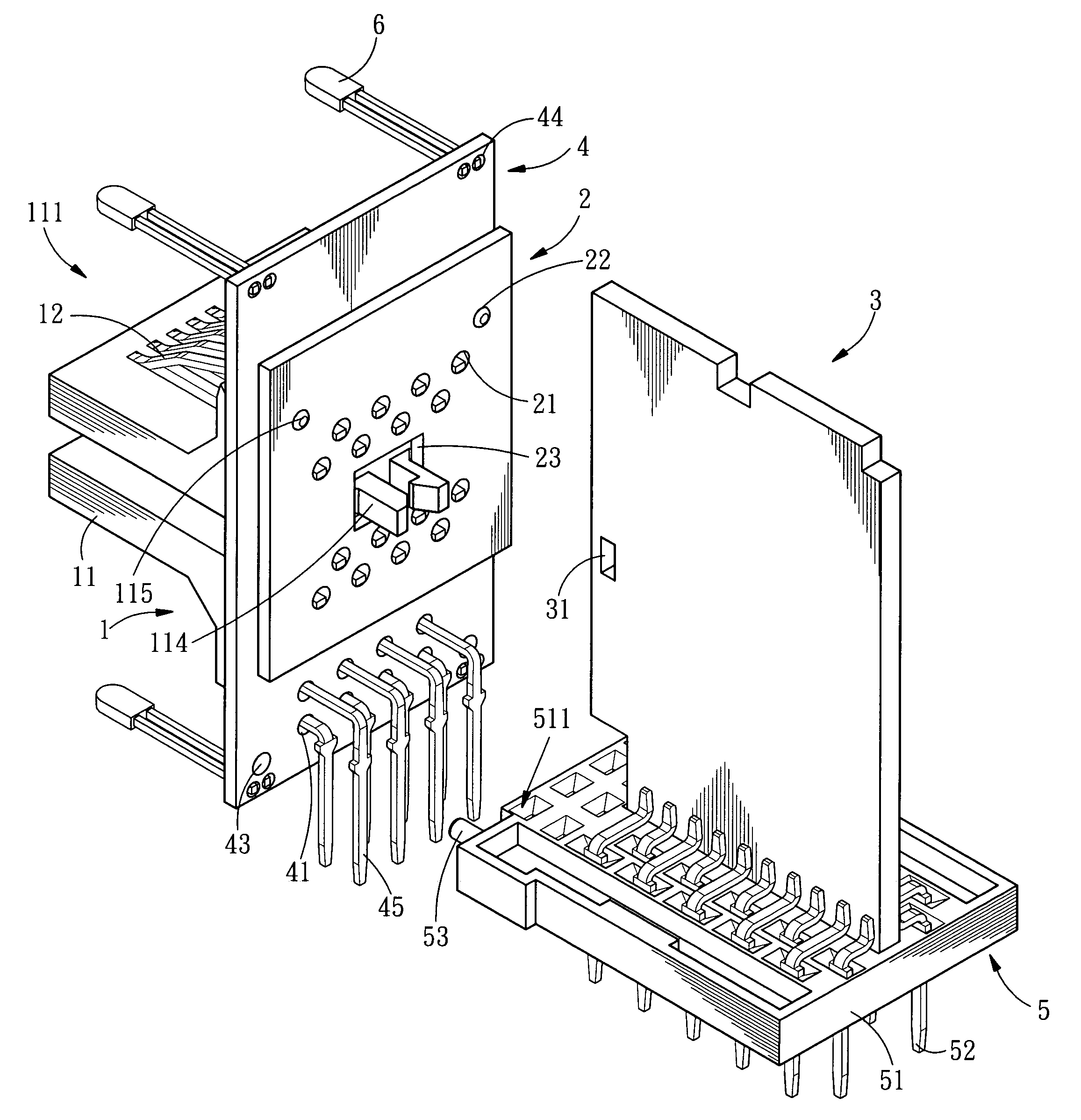
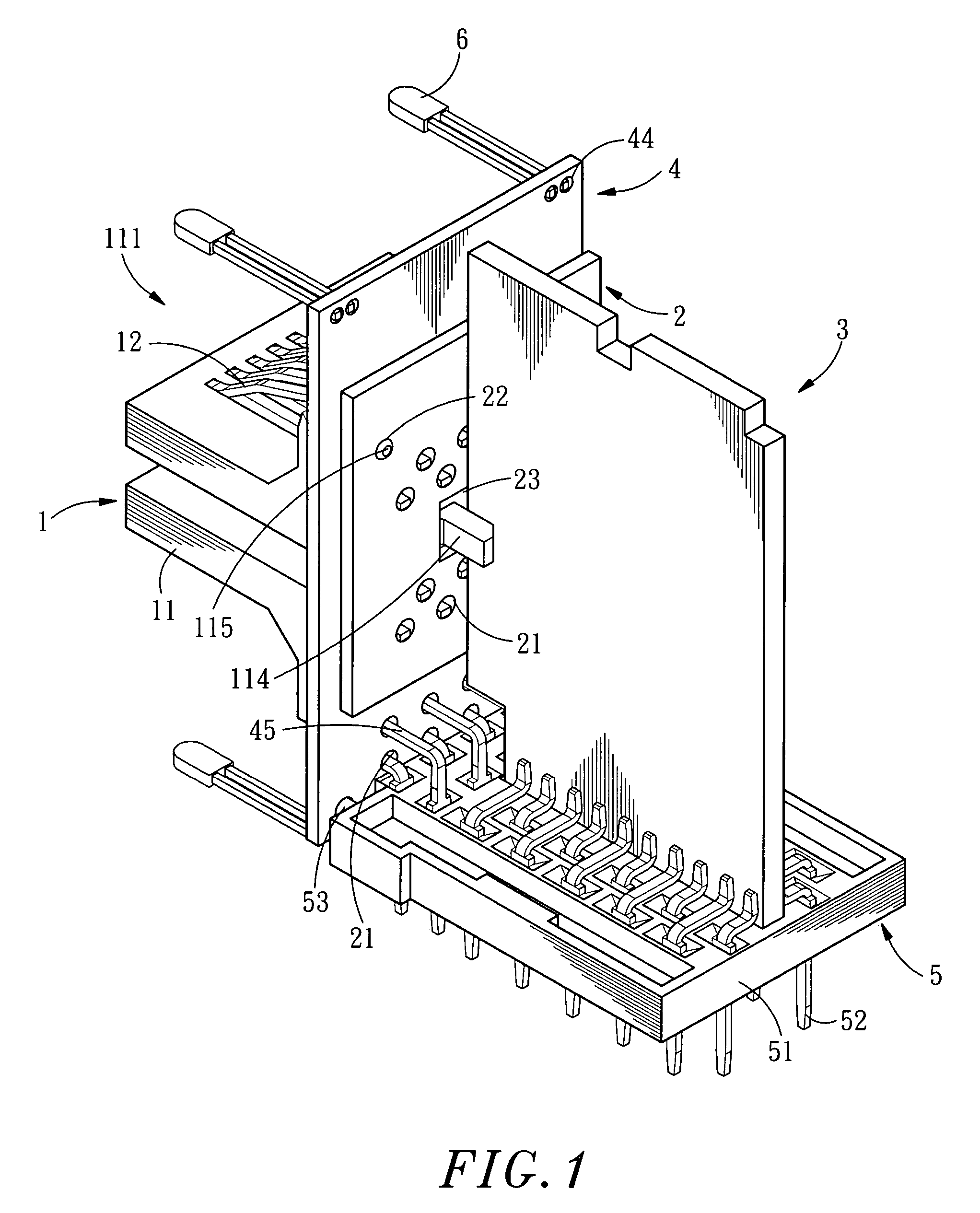
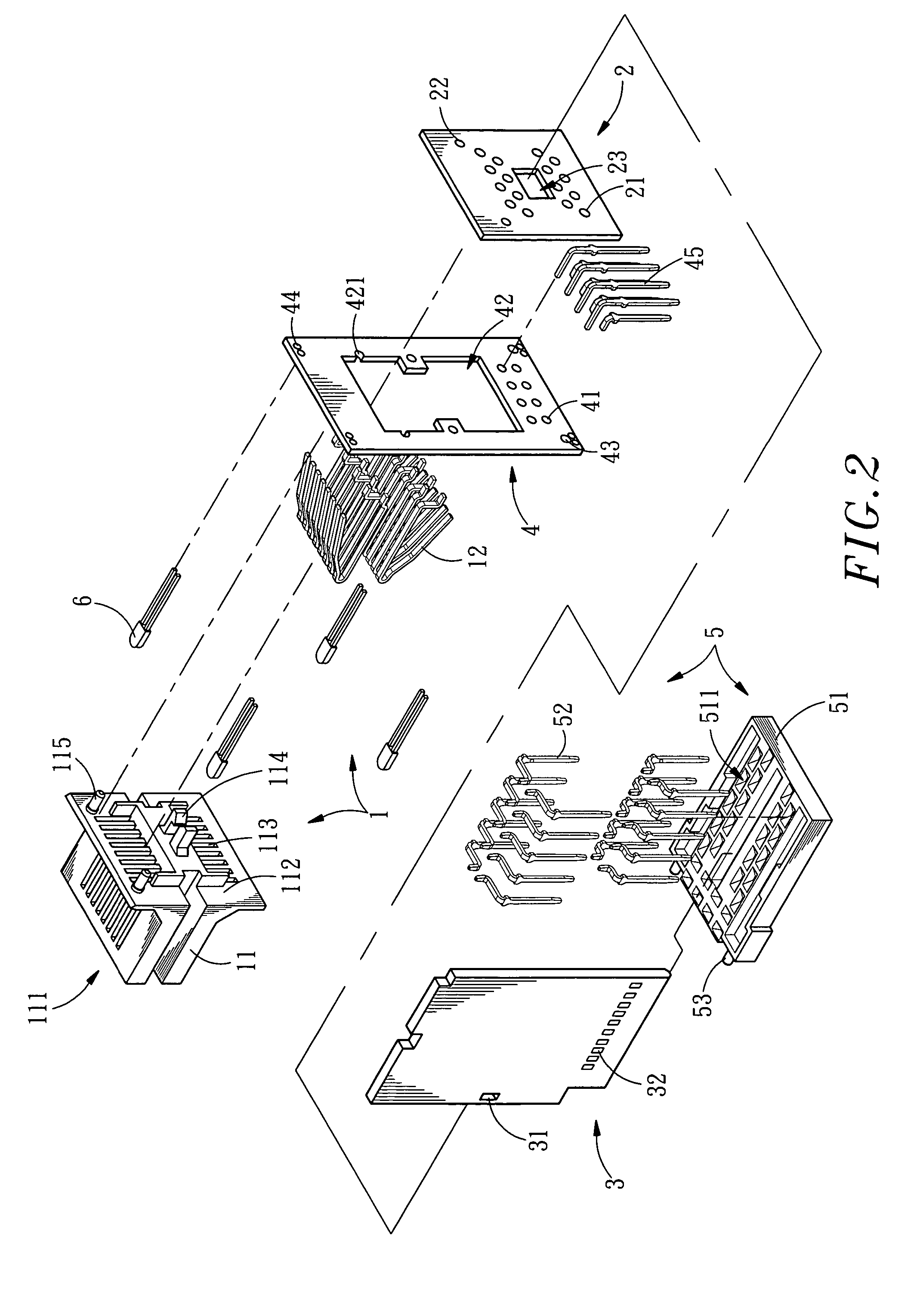
[0016]Referring to FIGS. 1, 2 and 3, the connector according to an embodiment of the present invention comprises an inserting module 1, a first circuit board 2, a second circuit board 3, a third circuit board 4, an adaptor module 5 and light-emitting diodes 6.

[0017]The inserting module 1 comprises a terminal set 11 and a plurality of terminals 12. The terminal set 11 comprises an inserting portion 111 formed at a side hereof and a receiving portion 112 formed at another side opposed to the inserting portion 111 thereof. The receiving portion 112 comprises a plurality of through slits 113, which are through the terminal set 11, connecting to the inserting portion 111 and two corresponding outwardly protruding hoo...


PUM


Abstract

A connector for reducing electro-manetic wave interference has a receiving module, a first circuit board, a second circuit board, a third circuit board and adaptor module. The circuits of various characteristics are set onto the first circuit board and the second circuit board respectively for reducing electro-magnetic wave interferences during signal transmission.

Description

BACKGROUND OF THE INVENTION[0001]1. The Field of the Invention[0002]The present invention relates to a structure of a connector, and more particularly to a structure of a connector comprising circuits having various electrical characteristics placed on different circuit boards for reducing electro-magnetic wave interference generated during the signal transmission.[0003]2. Description of Related Art[0004]The rapid advancement of computer technology has led to wide use of desktop computers or notebook computers. The user can use the computer to link up to the Internet to retrieve / transmit data. Therefore network technology provides convenience for accessing / transmitting information, which has become indispensable. Accordingly, the computer needs a connector for connecting to the Internet adaptor, and generally such connector is a RJ45. An RJ45 connector is generally used in connecting a computer to a Local Area Network (LAN) or connecting an Integrated Services Digital Network (ISDN)...

Claims


Application Information

Patent Timeline
Patent Type & Authority Patents(United States)
IPC IPC(8): H01R13/66H01R13/719
CPCH01R13/719H01R13/6581Y10S439/941H01R24/64
Inventor CHANG, CHIH-KAI
Owner SPEED TECH
Why Eureka
Try Eureka