Plating uniformity control by contact ring shaping

Inactive Publication Date: 2006-04-11
APPLIED MATERIALS INC
View PDF40 Cites 14 Cited by
  • Summary
  • Abstract
  • Description
  • Claims
  • Application Information

AI Technical Summary

Problems solved by technology

However, as the interconnect sizes decrease and aspect ratios increase, void-free interconnect feature fill via conventional metallization techniques becomes increasingly difficult.
Unfortunately, along with this increased current path comes

Method used


Image

  • Plating uniformity control by contact ring shaping
  • Plating uniformity control by contact ring shaping
  • Plating uniformity control by contact ring shaping

Examples


Embodiment Construction

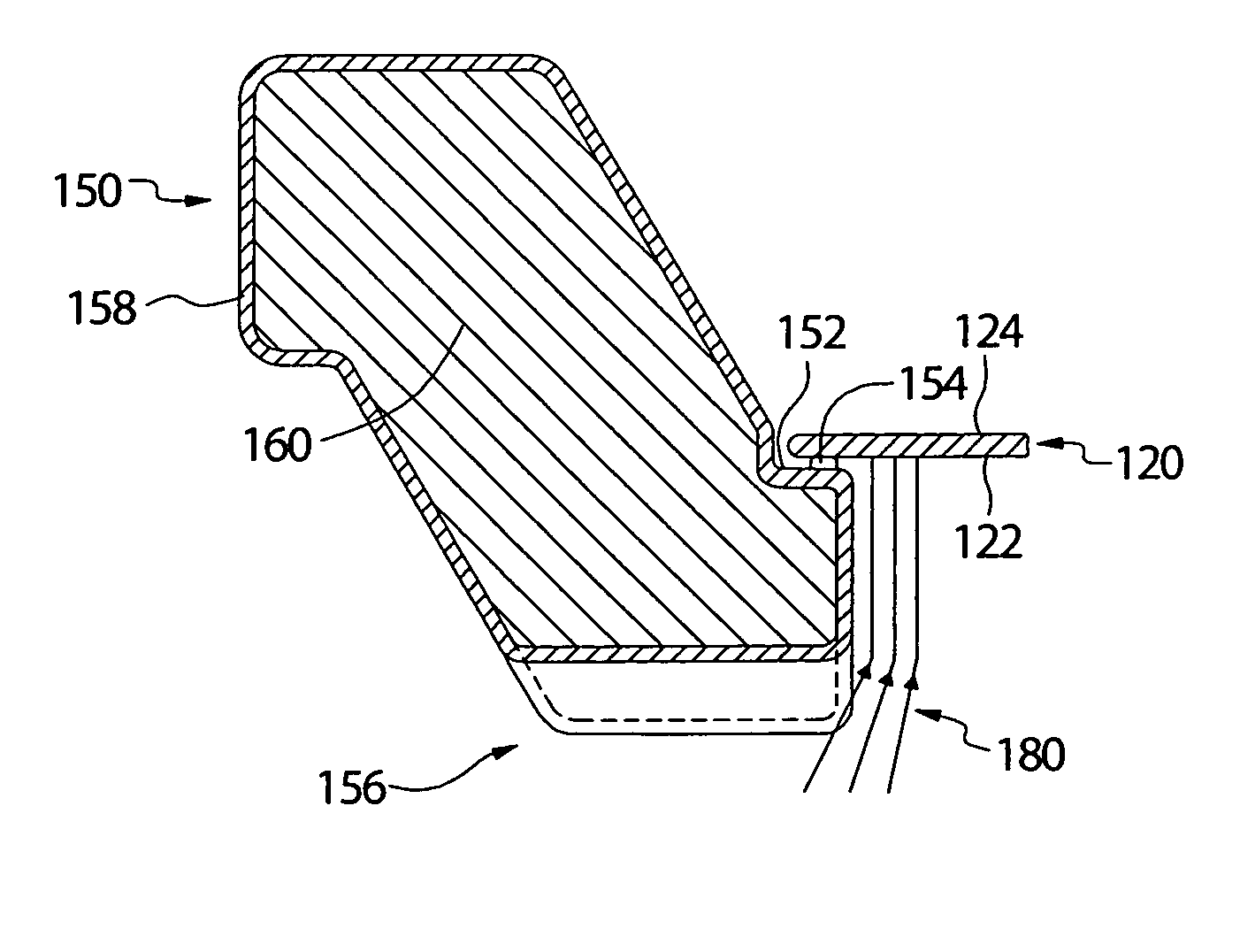
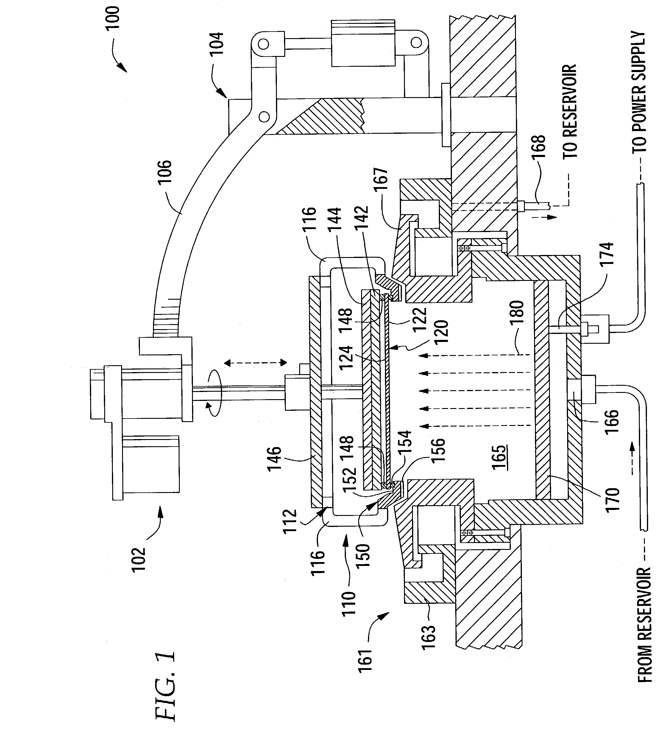
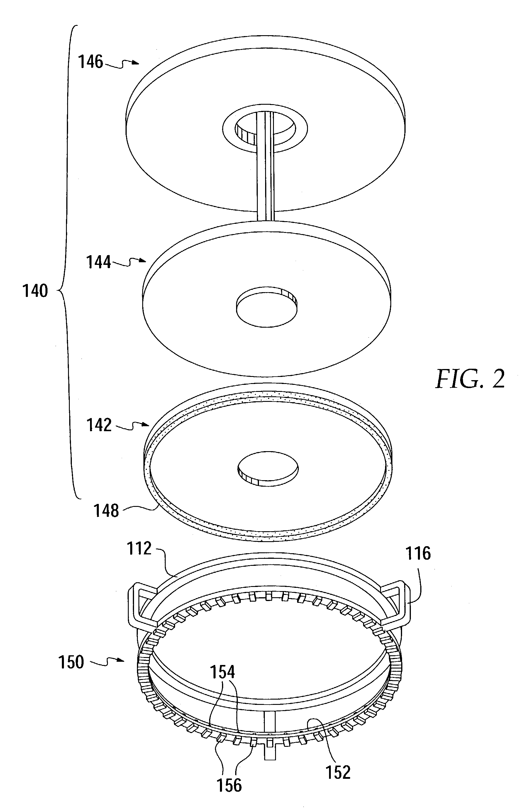
[0017]According to some aspects of the present invention, a contact ring having a plurality of electrical contacts is provided to supply an electrical bias to a substrate in a processing system. An average thickness of the contact ring may be increased via protrusions, or “scallops,” formed in the contact ring below the contacts. The scallops may help control variations in current density between the contacts by compensating for increased seed layer resistance that exists between the contacts.

[0018]As used herein, the term scallop generally refers to portions of a contact ring having an increased thickness at or near the contacts relative to (thinner) portions of the contact ring in between the contacts. For example, scallops may be formed on a bottom surface of a contact ring, below electrical contacts. Further, as used herein, top and bottom are relative terms, not limited to any specific orientation, generally applying to portions of a contact ring away from (top) or facing (bott...


PUM

PropertyMeasurementUnit
Thicknessaaaaaaaaaa
Thicknessaaaaaaaaaa
Thicknessaaaaaaaaaa

Abstract

An apparatus for providing an electrical bias to a substrate in a processing system is described. The apparatus generally includes a conductive annular body defining a central opening. The conductive annular body may have a substrate seating surface adapted to receive the substrate and a plurality of scallops formed on a surface opposing the substrate seating surface. A plurality of electrical contacts may be formed on the substrate seating surface opposite the plurality of scallops. The electrical contacts may be adapted to engage a plating surface of the substrate.

Description

BACKGROUND OF THE INVENTION[0001]1. Field of the Invention[0002]Embodiments of the invention generally relate to electrochemical plating and, more particularly, to a contact ring for providing an electrical bias to a substrate during an electrochemical plating process.[0003]2. Description of the Related Art[0004]Metallization of sub-quarter micron sized features is a foundational technology for present and future generations of integrated circuit manufacturing processes. More particularly, in devices such as ultra large scale integration-type devices, i.e., devices having integrated circuits with more than a million logic gates, the multilevel interconnects that lie at the heart of these devices are generally formed by filling high aspect ratio (greater than about 4:1, for example) interconnect features with a conductive material, such as copper or aluminum, for example. Conventionally, deposition techniques such as chemical vapor deposition (CVD) and physical vapor deposition (PVD)...

Claims


Application Information

Patent Timeline
IPC IPC(8): C25B9/00C25D7/12C25D17/06H01L21/288
CPCC25D17/06C25D7/123H01L21/2885Y10T29/5313Y10T29/49117Y10T29/49204Y10T29/532C25D17/001C25D5/18C25D17/005C25D17/007
Inventor HERCHEN, HARALDHAO, HENANESTEBAN, CELINA M.WEBB, TIMOTHY R.TRINH, SON N.
Owner APPLIED MATERIALS INC
Why Eureka
Try Eureka