Spatial light modulator, spatial light modulator array, and image formation apparatus

a technology of spatial light and modulator array, applied in the field of spatial light modulator, spatial light modulator array, image formation apparatus, can solve the problems of unsuitable miniaturization, achieve the effect of suppressing the manufacturing cost of optical function film, simple control of transmission and reflection of light, and strong incidence angle dependen

Inactive Publication Date: 2006-04-11
FUJIFILM CORP +1
View PDF4 Cites 42 Cited by
  • Summary
  • Abstract
  • Description
  • Claims
  • Application Information

AI Technical Summary

Benefits of technology

[0008]According to the configuration, the optical function film is inclined by applying voltage to the first electrode and the second electrode and thus as incident light from the light source is made incident on the optical function film, the incidence angle of the incident light changes in response to the inclination and the transmittance of the incident light changes accordingly. Therefore, a transmission spatial light modulator can be provided in the simple configuration. Since the restrictions on the optical path can be lessened, it is made possible to miniaturize the spatial light modulator.
[0011]According to the configuration, the light reflected on the optical function film can be prevented from becoming stray light and transmission and reflection of light can also be controlled with good accuracy. It is also made possible to degrade the creation accuracy of the spatial light modulator.
[0018]According to the configuration, deformation of the deformable member can be controlled using the electrostatic force occurring between the first and second electrodes and the electrostatic force occurring between the second and third electrodes, so that it is made possible to perform light modulation at high speed.
[0021]According to the configuration, the manufacturing cost of the optical function film can be suppressed. Since the cholesteric liquid crystal layer has strong incidence angle dependency, transmission and reflection of light can be controlled simply by changing a little the inclination angle of the optical function film, and the design flexibility of the spatial light modulator can be enhanced.

Problems solved by technology

A reflection spatial light modulator involves a problem of complicating the configuration of a peripheral optical system because incident light and outgoing light are on the same side relative to the spatial light modulator, and is unsuitable for miniaturization.

Method used


Image

  • Spatial light modulator, spatial light modulator array, and image formation apparatus
  • Spatial light modulator, spatial light modulator array, and image formation apparatus
  • Spatial light modulator, spatial light modulator array, and image formation apparatus

Examples


first embodiment

(First Embodiment)

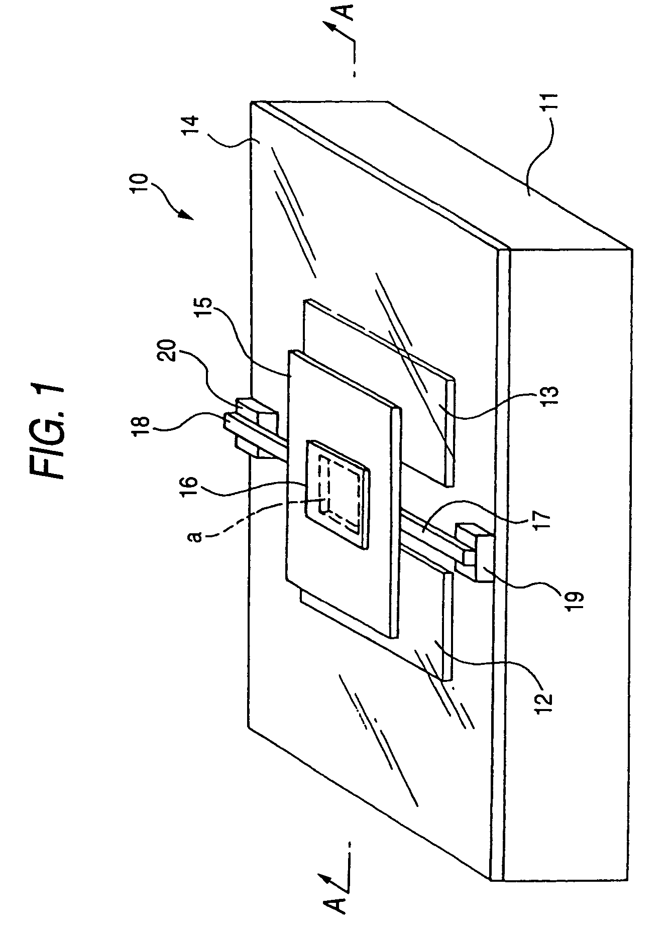
[0041]FIG. 1 is a perspective view to show a schematic configuration of a spatial light modulator to describe a first embodiment of the invention. The spatial light modulator of the embodiment is used with an image formation apparatus of an exposure device, a projector, a display, etc., and is manufactured by MEMS (Micro Electro Mechanical System).

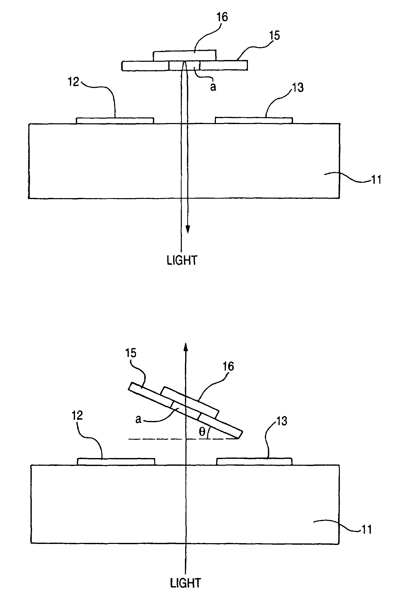
[0042]A spatial light modulator 10 includes a plane substrate 11, electrodes 12 and 13 provided on the plane substrate 11, an insulating film 14 formed on the electrodes 12 and 13, an electrode 15 placed above the electrodes 12 and 13 with a given space, an optical function film 16 formed on the surface of the electrode 15, hinge parts 17 and 18 for rotatably supporting the electrode 15, and support parts 19 and 20 for supporting the hinge parts 17 and 18.

[0043]The plane substrate 11 is made of a transparent member for incident light from a light source incident from below upward in FIG. 1 and is a glass substrate, etc., ...

second embodiment

(Second Embodiment)

[0096]FIG. 8 is a perspective view to show a schematic configuration of a spatial light modulator to describe a second embodiment of the invention. Components similar to those previously described with reference to FIG. 1 are denoted by the same reference numerals in FIG. 8 and will not be discussed again.

[0097]A spatial light modulator 26 includes a plane substrate 11, electrodes 12 and 13 provided on the plane substrate 11, an insulating film 14 formed on the electrodes 12 and 13, an electrode 15 placed above the electrodes 12 and 13 with a given space, an optical function film 16 formed on the surface of the electrode 15, hinge parts 17 and 18 for rotatably supporting the electrode 15, support parts 19 and 20 for supporting the hinge parts 17 and 18, electrodes 21 and 22, and support parts 23 and 24 for supporting the electrodes 21 and 22.

[0098]The support parts 23 and 24 are placed upright on the plane substrate 11 for supporting the electrodes 21 and 22 respe...

third embodiment

(Third Embodiment)

[0102]FIG. 9 is a perspective view to show a schematic configuration of a spatial light modulator to describe a third embodiment of the invention. The spatial light modulator of the embodiment is used with an image formation apparatus of an exposure device, a projector, a display, etc., and is manufactured by MEMS (Micro Electro Mechanical System).

[0103]A spatial light modulator 30 includes a plane substrate 31, a transparent electrode 32 provided on the plane substrate 31, a deformable member 35 having a thin film beam 34 placed above the transparent electrode 32 and a transparent electrode 33 formed covering the full surface of the thin film beam 34, and an optical function film 36.

[0104]The plane substrate 31 is made of a transparent member for incident light from a light source incident from below upward in FIG. 9 and is a glass substrate, etc., for example. The light from the light source passes through the plane substrate 31 and then passes through the thin f...


PUM

PropertyMeasurementUnit
thicknessaaaaaaaaaa
thicknessaaaaaaaaaa
wavelengthaaaaaaaaaa

Abstract

A spatial light modulator for changing transmittance of incident light from a light source to perform light modulation, the spatial light modulator comprising: a plane substrate transparent for the incident light; a first electrode being provided on the plane substrate; a deformable member being provided above the plane substrate and containing a second electrode placed with a gap above said first electrode, the deformable member deforming in response to an electrostatic force occurring as voltage is applied to said first electrode and the second electrode; and an optical function film being formed on the deformable member, wherein the optical function film has incidence angle dependency that the transmittance of the incident light changes in response to an incidence angle of the incident light on the optical function film, and is inclinable relative to the plane substrate in response to the electrostatic force.

Description

BACKGROUND OF THE INVENTION[0001]1. Field of the Invention[0002]This invention relates to a spatial light modulator for changing the transmittance of incident light from a light source for performing light modulation, a spatial light modulator array having the spatial light modulators put into an array, and an image formation apparatus using the spatial light modulator array.[0003]2. Description of the Related Art[0004]Hitherto, a DMD (Digital Micromirror Device) has been known as a device for forming an image. The DMD is as follows: An integrated circuit is formed on a silicon substrate, as many mirrors each having a minute size as the number of pixels are placed on the integrated circuit, and the reflection amount of light applied to the mirrors from a light source, thereby performing light modulation for forming an image. A document relevant to the DMD is JP-A-8-334709.[0005]The DMD is a device for reflecting light on a mirror, thereby performing light modulation. A reflection sp...

Claims


Application Information

Patent Timeline
Patent Type & Authority Patents(United States)
IPC IPC(8): G02B26/00G03B21/28G02F1/03G02B26/02G02F1/07G02F1/13G02F1/137G03F7/20H01L21/027
CPCG03F7/70291G02B26/0841
Inventor MOCHIZUKI, FUMIHIKO
Owner FUJIFILM CORP
Why Eureka
Try Eureka