Via-filling material and process for fabricating semiconductor integrated circuit using the material
a technology of semiconductor integrated circuit and material, which is applied in the direction of semiconductor/solid-state device manufacturing, basic electric elements, electric devices, etc., can solve the problems of inferior corrosion resistance of copper and disconnection in the fabricated semiconductor integrated circui
- Summary
- Abstract
- Description
- Claims
- Application Information
AI Technical Summary
Benefits of technology
Problems solved by technology
Method used
Image

Examples
embodiment 1
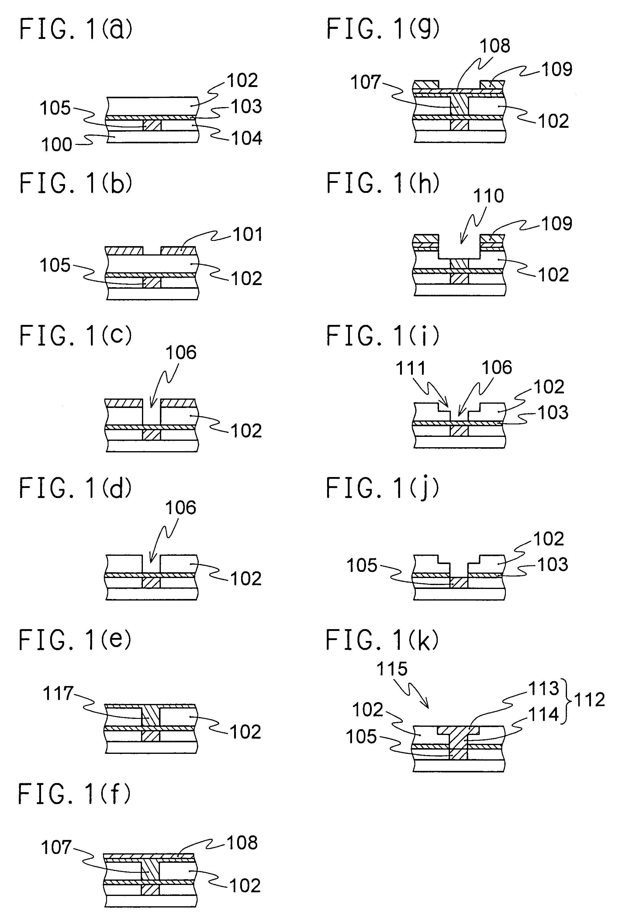
[0023]FIG. 1 is a cross-sectional view illustrating the steps of fabricating a semiconductor integrated circuit of Embodiment 1 using the via-filling material of the present invention, according to the via-first dual damascene process.
[0024]Referring to FIG. 1, lower insulating film 104 is formed on semiconductor substrate 100 and lower metal line 105 which is the first conductor is buried in this lower insulating film 104. Then upper insulating film 102 is laminated on the surface of lower insulating film 104 and metal line 105, interposing etching stopper film 103 therebetween (FIG. 1(a)).
[0025]In this embodiment, SiOC is used for lower insulating film 104 and upper insulating film 102 while silicone oxide insulating materials such as SiO2 and SiOF or organic spin-on-glass insulating materials such as SilK (available from Dow-Chemical Co. Ltd.) can also be used. On the other hand, silicone nitride films such as SiN and SiON are used for etching stopper film 103.
[0026]As the next s...
embodiment 2
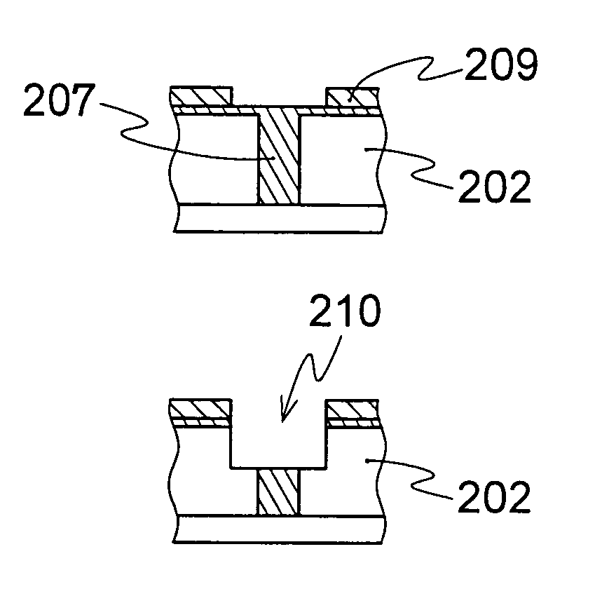
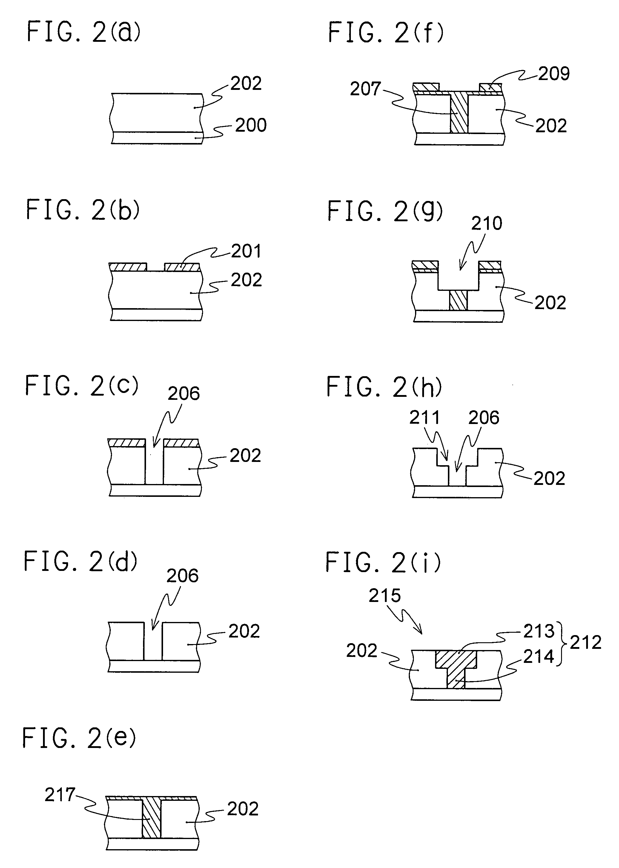
[0042]FIG. 2 is a cross-sectional view illustrating the steps of fabricating a semiconductor integrated circuit of Embodiment 2 using the via-filling material of the present invention, according to the via-first dual damascene process.
[0043]In FIG. 2, insulating film 202 is formed on semiconductor substrate 200 (FIG. 2(a)) and resist pattern 201 is formed on this insulating film 202 (FIG. 2(b)). Via hole 206 is created in insulating film 202 (FIG. 2(c)), followed by removal of resist pattern 201 (FIG. 2(d)). Thereafter via hole 206 is filled with via-filling material 217 (FIG. 2(e)). The via-filling material 217 used here is the same as that used in Embodiment 1.
[0044]Next, resist pattern 209 is formed on the via-filling body 207 obtained by solidifying via-filling material 217 existing on and leveling off insulating film 202 (FIG. 2(f)), insulating film 202 and via-filling body 207 are subjected to plasma etching with this resist pattern 209 as an etching mask and trench 210 is cre...
embodiment 3
[0046]This embodiment is carried out in the same manner as in Embodiment 1 except for using as via-filling material 117 a material comprising a copolymer of the first monomer represented by the formula (2):
[0047]
wherein R1 is a member selected from the group consisting of hydrogen atom, fluorine atom, chlorine atom, bromine atom and methyl group; R2 is a member selected from the group consisting of hydrogen atom, C1-3 alkyl group and C1-4 alkyl group in which the hydrogen atom is substituted by at least one kind of atoms of fluorine, chlorine and bromine atoms; and X is —C(═O)O— or —S(═O)2O—, and the second monomer which is an unsaturated compound containing an unsaturated group which brings about a copolymerization reaction with the first monomer and a functional group capable of crosslinking the copolymer.
[0048]In this embodiment, an unsaturated compound containing at least two unsaturated groups is particularly used as the second monomer.
[0049]Examples of the unsaturated compound...
PUM
| Property | Measurement | Unit |
|---|---|---|
| pressure | aaaaa | aaaaa |
| temperature | aaaaa | aaaaa |
| pore size | aaaaa | aaaaa |
Abstract
Description
Claims
Application Information
 - R&D
- Intellectual Property
- Life Sciences
- Materials
- Tech Scout
- Unparalleled Data Quality
- Higher Quality Content
- 60% Fewer Hallucinations
Browse by: Latest US Patents, China's latest patents, Technical Efficacy Thesaurus, Application Domain, Technology Topic, Popular Technical Reports.
© 2025 PatSnap. All rights reserved.Legal|Privacy policy|Modern Slavery Act Transparency Statement|Sitemap|About US| Contact US: help@patsnap.com