Method for manufacturing crystalline semiconductor film and method for manufacturing thin film transistor

a technology of crystalline semiconductor film and manufacturing method, which is applied in the direction of transistors, semiconductor devices, electrical equipment, etc., can solve the problems of increasing steps and increasing costs, and achieve the effects of reducing the number of steps of chemical solution and gas treatment, reducing the cost, and reducing the time taken for crystallization and removal of the cap film

Inactive Publication Date: 2011-06-14
SEMICON ENERGY LAB CO LTD
View PDF43 Cites 2 Cited by
  • Summary
  • Abstract
  • Description
  • Claims
  • Application Information

AI Technical Summary

Benefits of technology

[0009]It is an object of the present invention to simplify a step of crystallization of a semiconductor film by forming a cap film over the semiconductor film and a step of removal of the cap film, and to shorten time that is needed for the steps of crystallization and removal of the cap film.
[0018]In accordance with a method for manufacturing a crystalline semiconductor film of the present invention, by laser crystallization with a femtosecond laser, crystallization of the semiconductor film and removal of the cap film can be carried out at the same time when laser crystallization is performed to the amorphous semiconductor film over which the cap film is formed. Therefore, a step of removing the cap film in a later step can be omitted, which contributes to reduction in cost.
[0019]By adjusting energy of a femtosecond laser, crystallization of the semiconductor film and removal of the cap film can be separately carried out in different steps. In such a case, after crystallization of the semiconductor film, only the cap film over the semiconductor film can be removed using the femtosecond laser. Accordingly, an etching step of the cap film in a later step is unnecessary, and the number of steps of treatment of chemical solutions and gases can be reduced. Note that a laser other than a femtosecond laser, for examples, high harmonics such as an excimer laser or a solid laser may be used for crystallization of the semiconductor film in this case. Furthermore, since crystallization of the semiconductor film and removal of the cap film can be concurrently carried out, time taken for the steps of crystallization and removal of the cap film can be shortened.

Problems solved by technology

A chemical solution such as HF is used in a wet etching method and an etching gas such as CF4 is used in a dry etching, and therefore, the cost is increased caused by increase of steps, and treatment of the chemical solution and gas is needed (for example, Reference 1: Japanese Published Patent Application No. 2000-228360).

Method used


Image

  • Method for manufacturing crystalline semiconductor film and method for manufacturing thin film transistor
  • Method for manufacturing crystalline semiconductor film and method for manufacturing thin film transistor
  • Method for manufacturing crystalline semiconductor film and method for manufacturing thin film transistor

Examples


embodiment mode 1

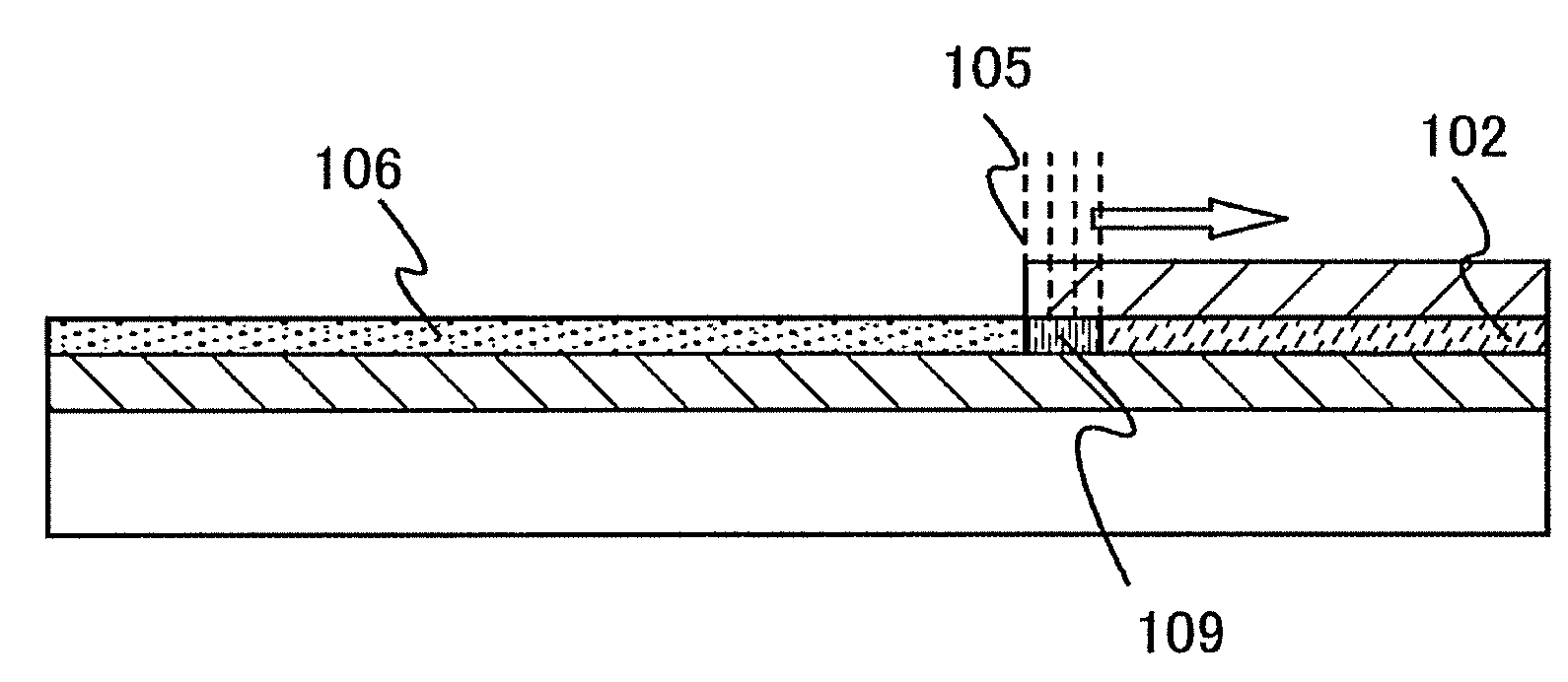
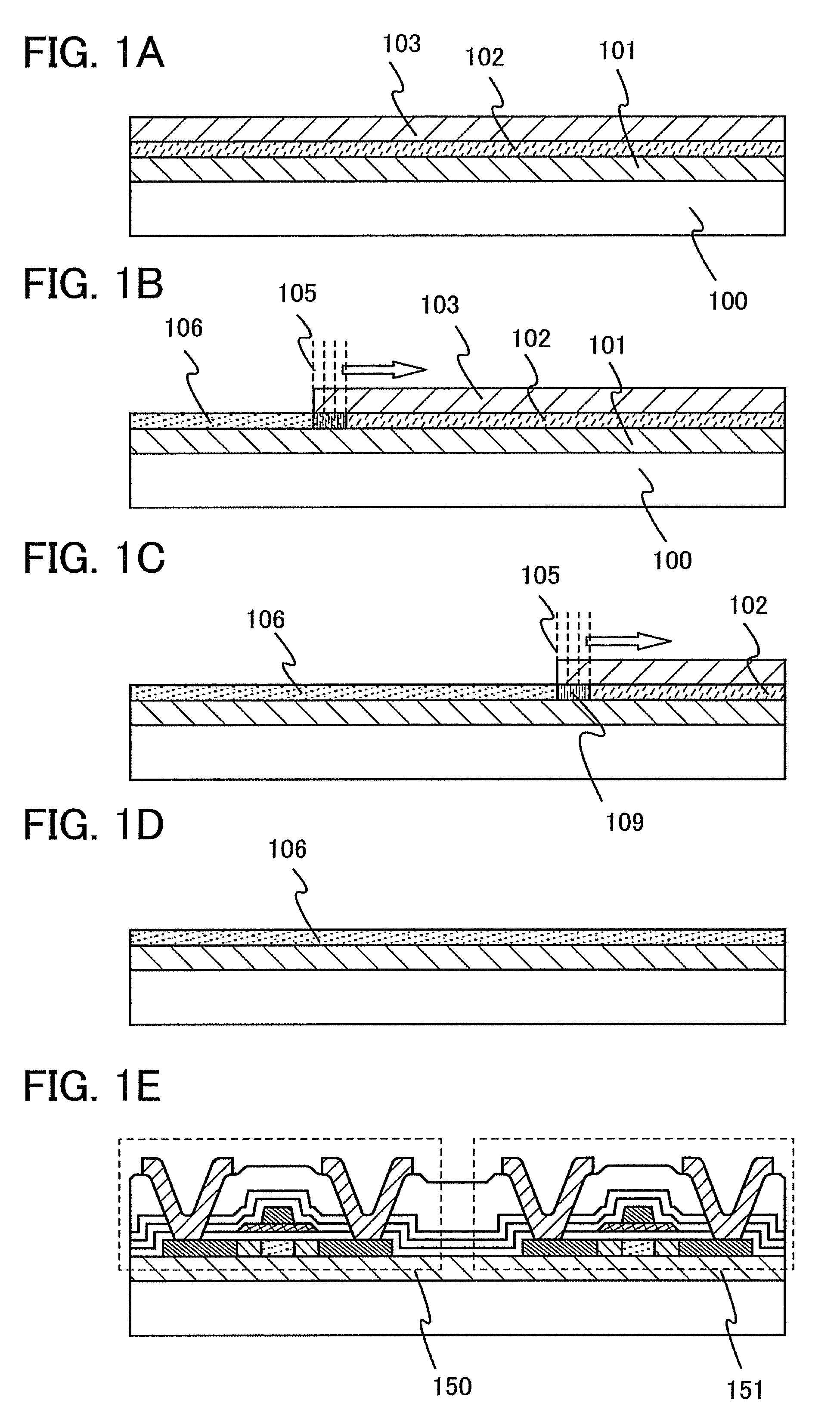
[0040]Hereinafter, a method for manufacturing a crystalline semiconductor film of the present invention and a method for manufacturing a thin film transistor using the crystalline semiconductor film will be described with reference to drawings. FIGS. 1A to 1E are diagrams illustrating a step of a manufacturing method of the present invention.

[0041]First, as shown in FIG. 1A, an insulating film 101 functioning as a base film is formed on one of surfaces of a substrate 100 having an insulating surface. The insulating film 101 functioning as a base film is formed using a silicon oxide film, a silicon nitride film, a silicon nitride oxide film containing a larger amount of nitrogen than that of oxygen, a silicon oxynitride film containing a larger amount of oxygen than that of nitrogen, each of which has a thickness of 50 to 150 nm, or the like as appropriate. Here, as the substrate 100 having an insulating surface, a glass substrate with a thickness of 0.7 mm is for example used. Furth...

embodiment mode 2

[0066]Hereinafter, another mode of a method for manufacturing a crystalline semiconductor film of the present invention and a method for manufacturing a thin film transistor using the crystalline semiconductor film will be described with reference to drawings. FIGS. 3A to 3E are diagrams illustrating a manufacturing method of the present invention.

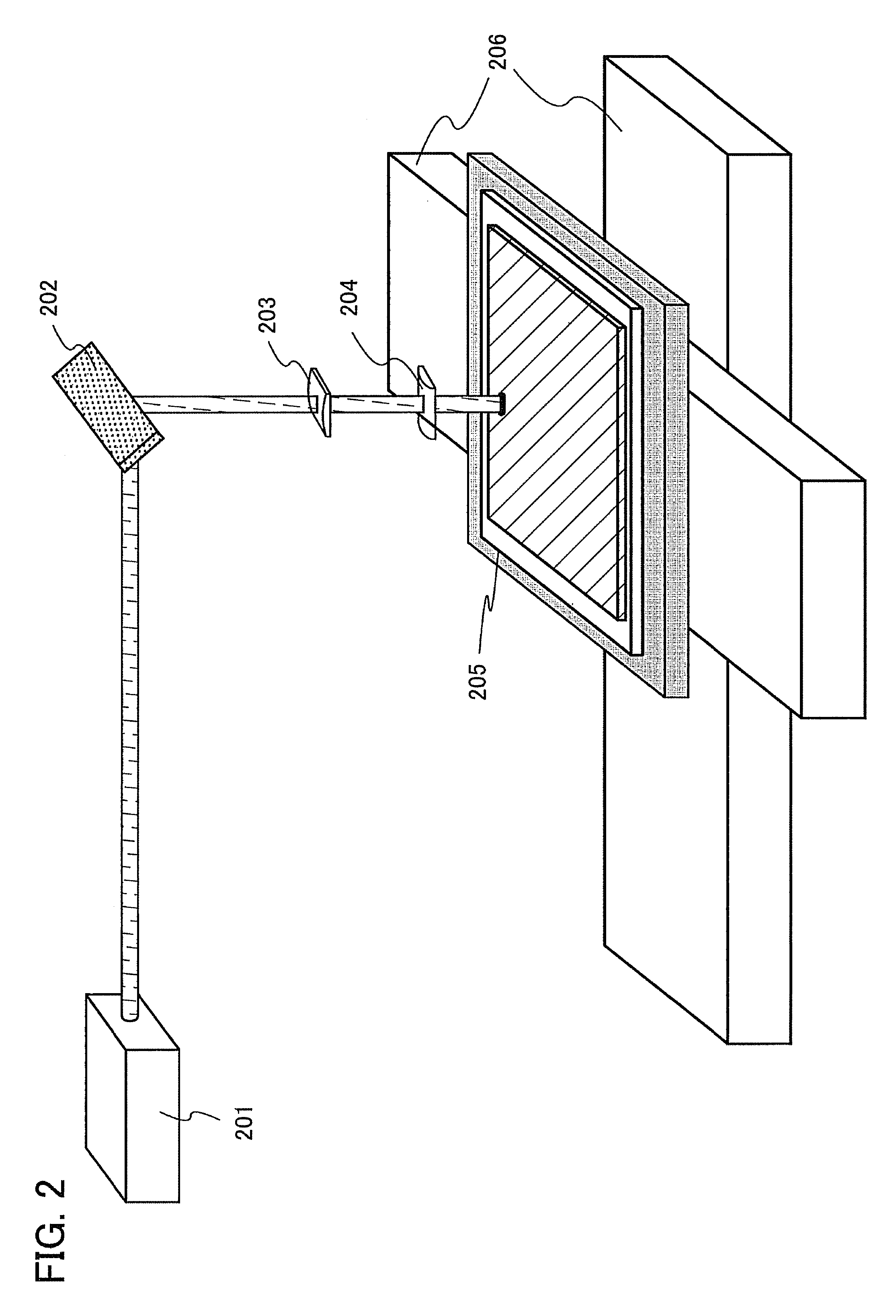
[0067]First, the substrate 100 is prepared, over which the insulating film 101, the semiconductor film 102, and the cap film 103 are sequentially formed by a described method with the use of FIG. 1A in Embodiment Mode 1. The substrate 100 is scanned by irradiation with a laser beam 110 for crystallization from above the cap film 103 as shown in FIG. 3A. As shown in FIGS. 3B and 3C, the substrate is irradiated in a scanning direction with a laser beam 111 of a femtosecond laser from behind the laser beam 110 for crystallization so that irradiation with the laser beam 111 is performed along with the irradiation with the laser beam 110. The s...

embodiment 1

[0082]This embodiment will describe an example in which crystallization of an amorphous semiconductor film and removal of a cap film are performed at the same time with the femtosecond laser used in the manufacturing method of a crystalline semiconductor thin film shown in Embodiment Mode 1 of the present invention, with reference to drawings.

[0083]First, samples were manufactured by a method described below. As a base film, a silicon nitride oxide film with a thickness of 50 nm was formed over a glass substrate by a plasma CVD method, and then, a silicon oxynitride film with a thickness of 100 nm was formed by a plasma CVD method. Next, an amorphous silicon film was formed over the base film by a plasma CVD method, and SiNO with a thickness of 300 nm was deposited as a cap film over the amorphous silicon film by a plasma CVD method. In such a manner, three kinds of amorphous silicon films with a thickness of 20 nm, 25 nm, and 30 nm as samples were manufactured. The SiNO contains Si...


PUM


Abstract

The present invention relates to a method for manufacturing a polycrystalline semiconductor film that can be used for a semiconductor device. In the method, an amorphous semiconductor film is irradiated with a femtosecond laser to be crystallized. By laser irradiation using a femtosecond laser, when an amorphous semiconductor film over which a cap film is formed is crystallized with a laser, it becomes possible to perform crystallization of the semiconductor film and removal of the cap film at the same time. Therefore, a step of removing the cap film in a later step can be omitted.

Description

BACKGROUND OF THE INVENTION[0001]1. Field of the Invention[0002]The present invention relates to a method for manufacturing a crystalline semiconductor film that can be used in a semiconductor device, by which an amorphous semiconductor film is irradiated with a laser to be crystallized, and a method for manufacturing a thin film transistor using the crystalline semiconductor film. Note that a semiconductor device in the present specification generally indicates a device capable of functioning by utilizing semiconductor characteristics, and electro-optic devices, semiconductor circuits, and electronic devices are all semiconductor devices.[0003]2. Description of the Related Art[0004]In recent years, it has been possible to form a liquid crystal display device provided with a driver circuit over a cheap glass substrate by crystalline silicon thin film transistors (TFT). As a method for forming a crystalline silicon thin film, a method can be given, in which an amorphous silicon film ...

Claims


Application Information

Patent Timeline
Patent Type & Authority Patents(United States)
IPC IPC(8): H01L29/786
CPCH01L21/02532H01L21/02686H01L29/66757H01L27/1285H01L21/02691H01L21/2026H01L27/1214
Inventor OMATA, TAKATSUGU
Owner SEMICON ENERGY LAB CO LTD
Why Eureka
Try Eureka