Light emitting device and electronic device

a technology of light emitting devices and electronic devices, applied in the field of electroluminescent light sources, can solve the problems of insufficient luminance difference between adjacent pixels, human eye hardly detects the difference in luminance between pixels apart from each other, and cannot be recognized by the human eye, so as to prevent crosstalk

Inactive Publication Date: 2006-04-18
SEMICON ENERGY LAB CO LTD
View PDF22 Cites 45 Cited by
  • Summary
  • Abstract
  • Description
  • Claims
  • Application Information

AI Technical Summary

Benefits of technology

[0043]The present invention has been made in view of the above and an object of the present invention is

Problems solved by technology

In this case, however, the difference in luminance between adjacent pixels is not great enough to be recognizable by the human eye.
Also, although the difference in luminance is the greatest between the nearest pixel to the power supply of a power supply

Method used


Image

  • Light emitting device and electronic device
  • Light emitting device and electronic device
  • Light emitting device and electronic device

Examples


embodiment mode 1

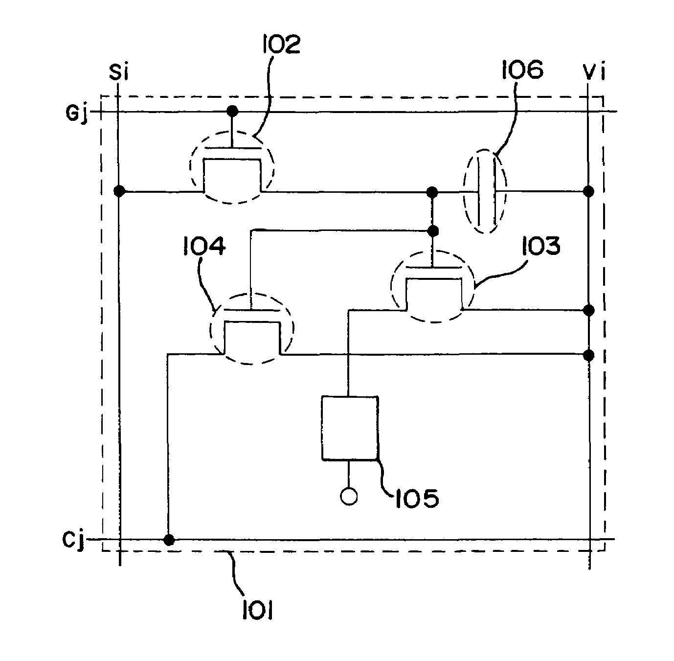
[0184]FIG. 1 shows the structure of a pixel in a light emitting device of the present invention. A plurality of pixels 101 are provided in a pixel portion of the light emitting device of the present invention. Each of the pixels 101 has a source signal line Si (one of source signal lines S1 to Sx), a power supply line Vi (one of power supply lines V1 to Vx), a gate signal line Gj (one of gate signal lines G1 to Gy), and a reference power supply line Cj (one of power supply lines G1 to Cy). Each of the pixels 101 also has a switching TFT 102, an EL driving TFT 103, an electric discharge TFT 104, an EL element 105, and a capacitor 106.

[0185]The polarity of the EL driving TFT 103 is reverse to the polarity of the electric discharge TFT 104. Accordingly, the electric discharge TFT 104 is a p-channel TFT when the EL driving TFT 103 is an n-channel TFT. On the other hand, the electric discharge TFT 104 is an n-channel TFT when the EL driving TFT 103 is a p-channel TFT.

[0186]A gate electro...

embodiment mode 2

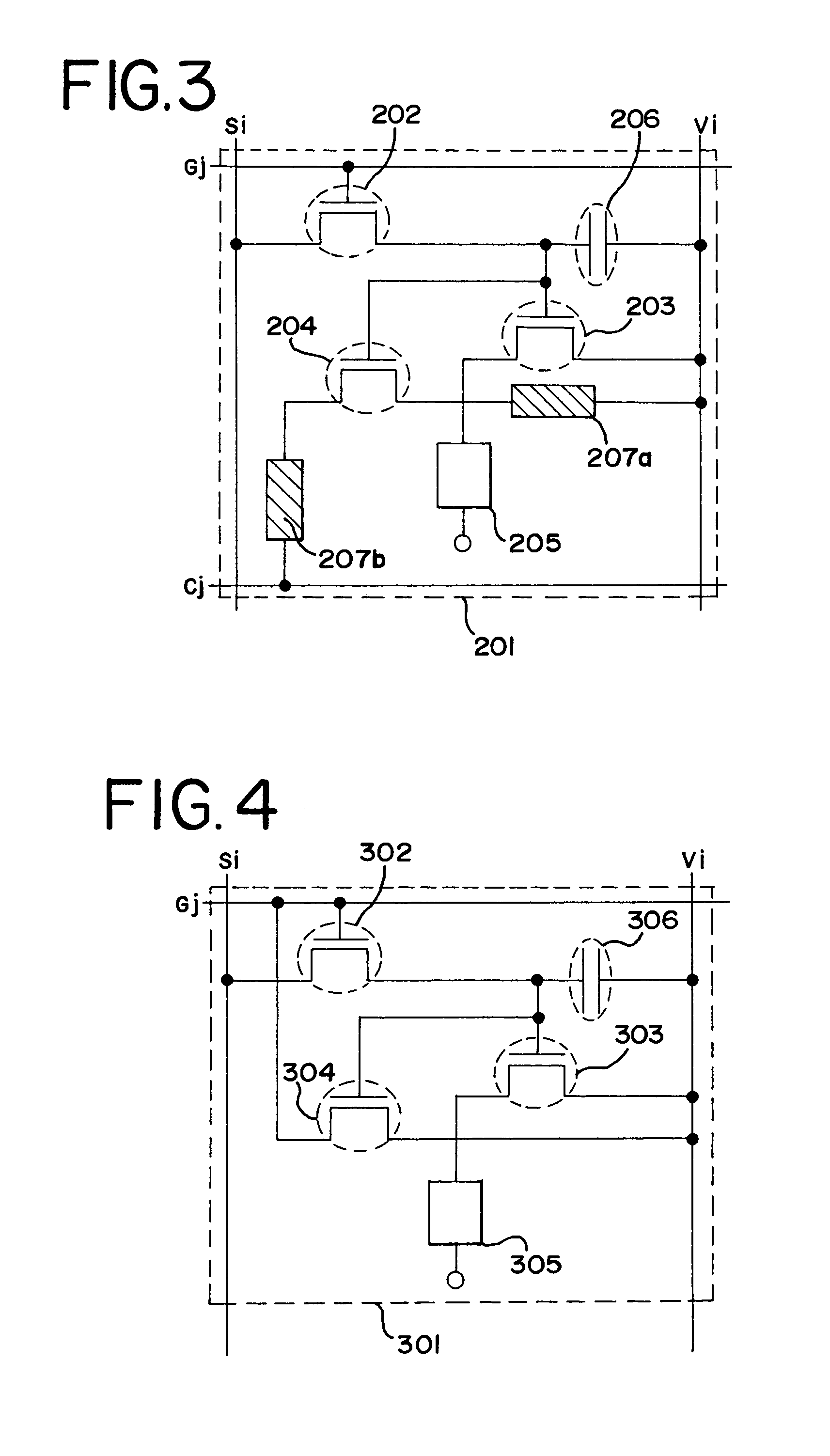
[0215]Described in this embodiment mode is about, in the pixel of the light emitting device shown in FIG. 1, providing a current controlling element between the source region or the drain region of the electric discharge TFT and the power supply line Vi, and also providing a current controlling element between the source region or the drain region of the electric discharge TFT and the reference power supply line Cj.

[0216]FIG. 3 shows the structure of a pixel according to this embodiment mode. A pixel 201 has a source signal line Si (one of source signal lines S1 to Sx), a power supply line Vi (one of power supply lines V1 to Vx), a gate signal line Gj (one of gate signal lines G1 to Gy), and a reference power supply line Cj (one of power supply lines G1 to Cy). The pixel 201 also has a switching TFT 202, an EL driving TFT 203, an electric discharge TFT 204, an EL element 205, a capacitor 206, and current controlling elements 207a and 207b.

[0217]As in the case of FIG. 1, the polarit...

embodiment mode 3

[0229]This embodiment mode describes the structure of the pixel in the light emitting device shown in FIG. 1 when the gate signal line Gj substitutes for the reference power supply line Cj.

[0230]FIG. 4 shows the structure of a pixel according to this embodiment mode. A pixel 301 has a source signal line Si (one of source signal lines S1 to Sx), a power supply line Vi (one of power supply lines V1 to Vx), and a gate signal line Gj (one of gate signal lines G1 to Gy). The pixel 301 also has a switching TFT 302, an EL driving TFT 303, an electric discharge TFT 304, an EL element 305, and a capacitor 306.

[0231]A gate electrode of the switching TFT 302 is connected to the gate signal line Gj. The switching TFT 302 has a source region and a drain region, one of which is connected to the source signal line Si and the other of which is connected to a gate electrode of the EL driving TFT 303 and to a gate electrode of the electric discharge TFT 304.

[0232]The capacitor 306 is placed between t...


PUM


Abstract

A TFT for controlling the amount of current flowing into a power supply line when an EL element does not emit light (electric discharge TFT) is provided in each pixel. When an EL driving TFT is turned ON to make an EL element emit light, the electric discharge TFT is turned OFF. On the other hand, the electric discharge TFT is turned ON when the EL driving TFT is turned OFF and no EL element emit light. Therefore variation of the difference in electric potential over the length of a power supply line depending on an image to be displayed is contained. Thus reduced is the difference in amount of current flowing into EL elements in adjacent pixels while the EL elements emit light, thereby avoiding crosstalk.

Description

BACKGROUND OF THE INVENTION[0001]1. Field of the Invention[0002]The present invention relates to an EL panel in which an EL element formed on a substrate is sealed between the substrate and a cover member. The invention also relates to an EL module with IC mounted to the EL panel. In this specification, the EL panel and the EL module are generically called light emitting devices. The present invention further relates to an electronic device employing the light emitting devices.[0003]2. Description of the Related Art[0004]Self-light emitting EL elements eliminate the need for a backlight that is necessary in liquid crystal displays (LCDs) and thus make it easy to manufacture thinner displays. Also, the EL elements are high in visibility and have no limit in terms of viewing angle. These are the reasons for attention that light emitting devices using the EL elements have been receiving recently as display devices to replace CRTs and LCDs.[0005]An EL element has a layer containing an o...

Claims


Application Information

Patent Timeline
IPC IPC(8): G09G3/36H05B44/00G09G3/20G09G3/32
CPCG09G3/3233G09G3/3696G09G3/2022G09G2300/0809G09G2300/0842G09G2300/0861G09G2320/0209G09G2320/0214G09G2320/0223G09G2320/0233G09G2330/021G09G2300/089
Inventor KIMURA, HAJIME
Owner SEMICON ENERGY LAB CO LTD
Why Eureka
Try Eureka