Method for manufacturing optical waveguide using laser direct writing method and optical waveguide manufactured by using the same

a manufacturing method and laser direct writing technology, applied in the field of manufacturing optical waveguides, can solve the problems of difficult implementation of sharpness in the boundary (between the core material and the clad material) of the photolithography method and achieve the effect of improving the refractive index profile of the optical waveguid

Inactive Publication Date: 2006-04-18
ELECTRONICS & TELECOMM RES INST
View PDF7 Cites 11 Cited by
  • Summary
  • Abstract
  • Description
  • Claims
  • Application Information

AI Technical Summary

Benefits of technology

[0014]Thus, in order to solve the above-mentioned problems, the object of the present invention is to provide a method of improving the refractive index profile of the optical waveguide, in the method for manufacturing the optical waveguide by using the laser direct writing method.
[0015]The another object of the present invention is to provide a method of improving the refractive index profile of the optical waveguide without an additional device such as the diffracting phase mask or the hologram in the donut mode beam, by overlapping two or more Gaussian beams to manufacture the optical waveguide.
[0016]The another object of the present invention is to provide a method of reducing a bending loss in the curved region of the optical waveguide through asymmetrical overlapping beams and a method for manufacturing a S-bending type optical waveguide having an offset structure.

Problems solved by technology

The photolithography method includes very complicate processes such as a step of coating a cladding material on a substrate, a step of baking, a step of coating a core material, a step of applying a photoresist, a step of exposing using a photomask, a step of developing and a step of etching.
However, in case the optical waveguide is implemented through the laser direct writing method according to prior art, it is difficult to implement a sharpness in boundary (between core material and clad material) of the optical waveguide, because of the nature of the light.

Method used


Image

  • Method for manufacturing optical waveguide using laser direct writing method and optical waveguide manufactured by using the same
  • Method for manufacturing optical waveguide using laser direct writing method and optical waveguide manufactured by using the same
  • Method for manufacturing optical waveguide using laser direct writing method and optical waveguide manufactured by using the same

Examples


Embodiment Construction

[0031]Hereinafter, the embodiments of the present invention will be explained with reference to the accompanying drawings. However, the embodiment of the present invention can be changed into a various type, and it should be not understood that the scope of the present invention is limit to the following embodiments. The embodiments of the present invention are provided in order to explain the present invention to those skilled in the art.

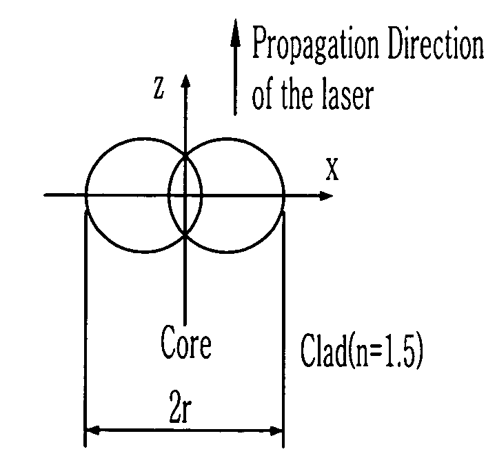
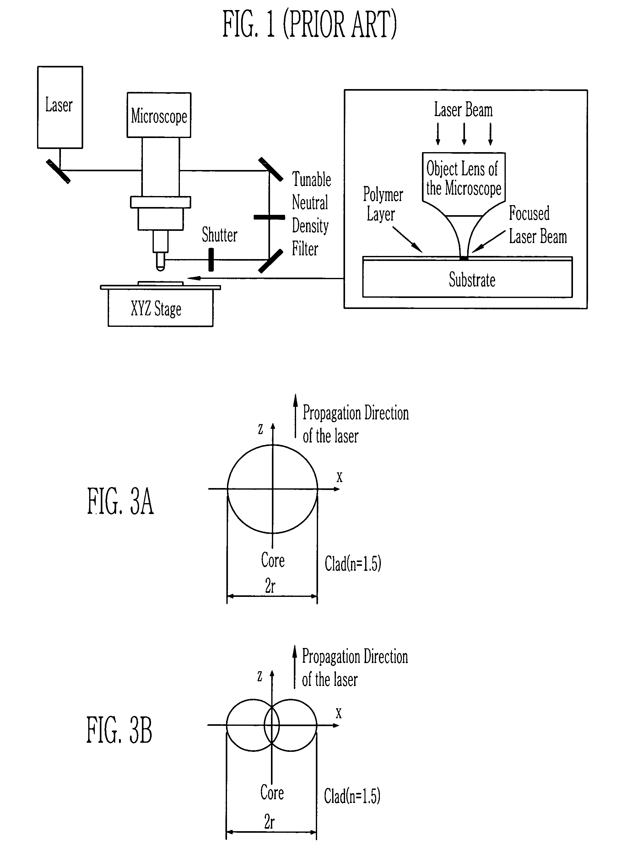
[0032]In manufacturing the optical waveguide, a clad material is coated on the plane substrate, and the photo-sensitive polymer is coated thereon as the core layer. For laser direct writing process, the laser beam is focused and irradiated on the core layer material and the size of the beam is adjusted to a desired size. The stage of substrate is moved to write the pattern of the optical waveguide. Alternatively, the laser beam may be moved. The refractive index of the exposed pattern becomes larger than that of the material, which not exposed, the...


PUM


Abstract

A method of manufacturing an optical waveguide using a laser direct writing method is disclosed. More particularly, a method for improving refractive index profile of the optical waveguide by overlapping two or more beams using Gaussian laser beam is provided. In addition, it can accomplish an improved waveguide characteristics such as an offset structure of an S-bend type optical waveguide and an asymmetrical curve optical waveguide by individually adjusting the overlapped laser beams.

Description

BACKGROUND OF THE INVENTION[0001]1. Field of the Invention[0002]The present invention relates to a method for manufacturing an optical waveguide by a direct writing method and the optical waveguide manufactured by using the same, and more particularly, to a method of improving a refractive index profile of the optical waveguide by overlapping two or more beams using a Gaussian laser. Also, the present invention provides a method for manufacturing the optical waveguide which is capable of improving waveguide characteristics such as offset structure of a S-bend type optical waveguide and an asymmetrical curved optical waveguide by individually adjusting each of the overlapped laser beams, independently.[0003]2. Description of the Prior Art[0004]The method for manufacturing the optical waveguide using the laser direct writing method has the procedure of focusing the laser beam on a photo-sensitive polymer in order to pass through a writing process and increasing the refractive index of...

Claims


Application Information

Patent Timeline
Patent Type & Authority Patents(United States)
IPC IPC(8): G02B6/10G02B6/12G02B6/125G02B6/138
CPCG02B6/138G02B6/125G02B6/12
Inventor LEE, WOO JINAHN, SEUNG HOYOON, KEUN BYOUNGJEONG, MYUNG YUNG
Owner ELECTRONICS & TELECOMM RES INST
Why Eureka
Try Eureka