Epitaxy/substrate release layer
a technology of substrate and epitaxial growth, applied in the direction of basic electric elements, electrical apparatus, semiconductor devices, etc., can solve the problems of poor thermal conduction, and achieve the effect of high electron mobility transistor and high electron mobility transistor
- Summary
- Abstract
- Description
- Claims
- Application Information
AI Technical Summary
Benefits of technology
Problems solved by technology
Method used
Image

Examples
Embodiment Construction
[0020]The embodiments set forth below represent the necessary information to enable those skilled in the art to practice the invention and illustrate the best mode of practicing the invention. Upon reading the following description in light of the accompanying drawing figures, those skilled in the art will understand the concepts of the invention and will recognize applications of these concepts not particularly addressed herein. It should be understood that these concepts and applications fall within the scope of the disclosure and the accompanying claims.
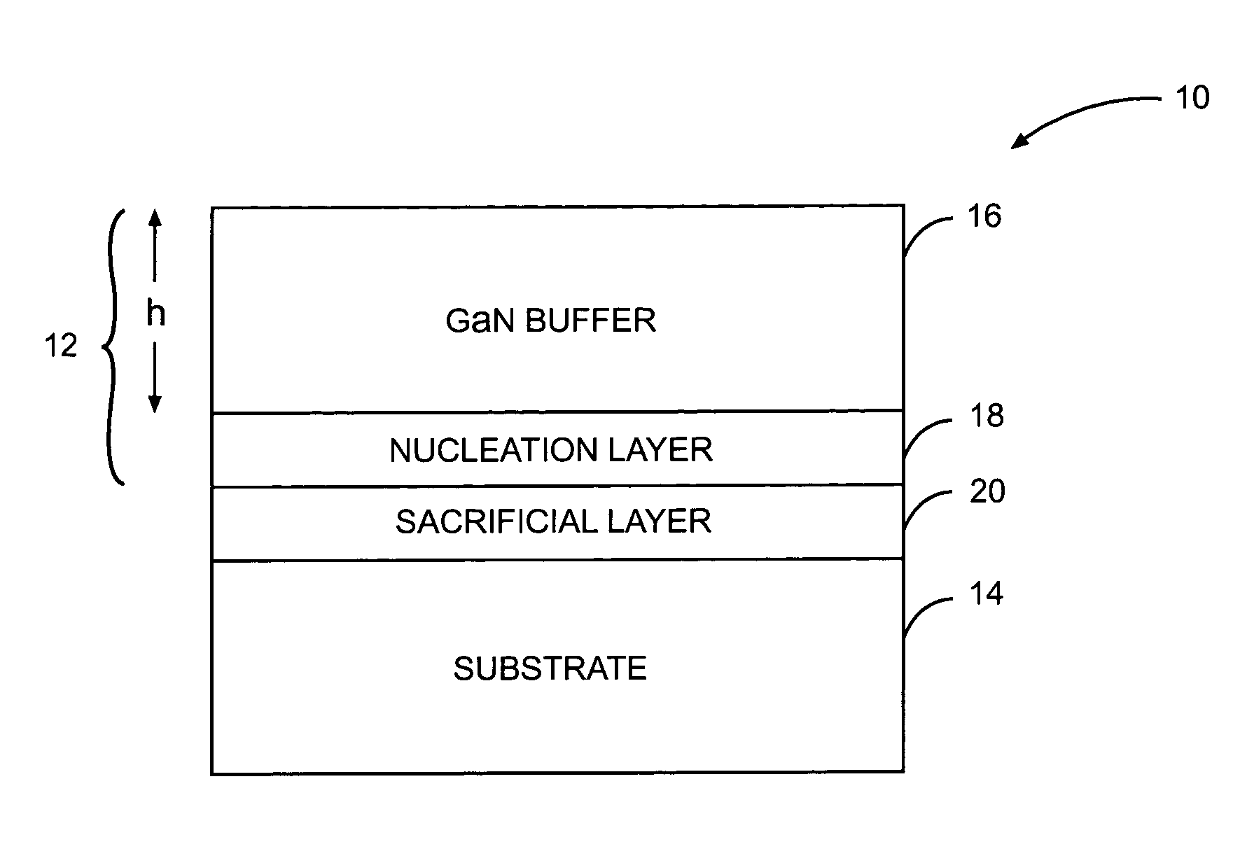
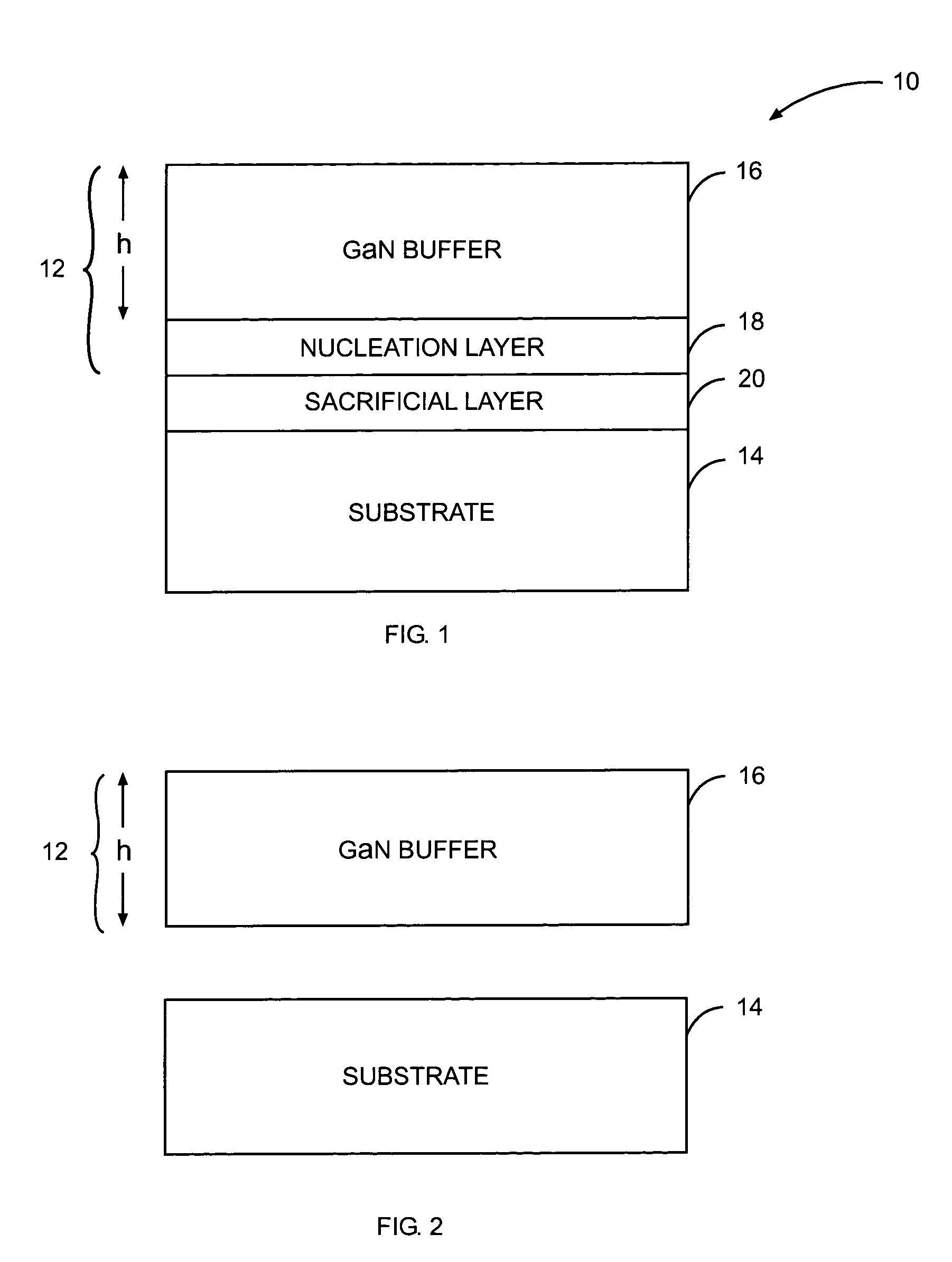
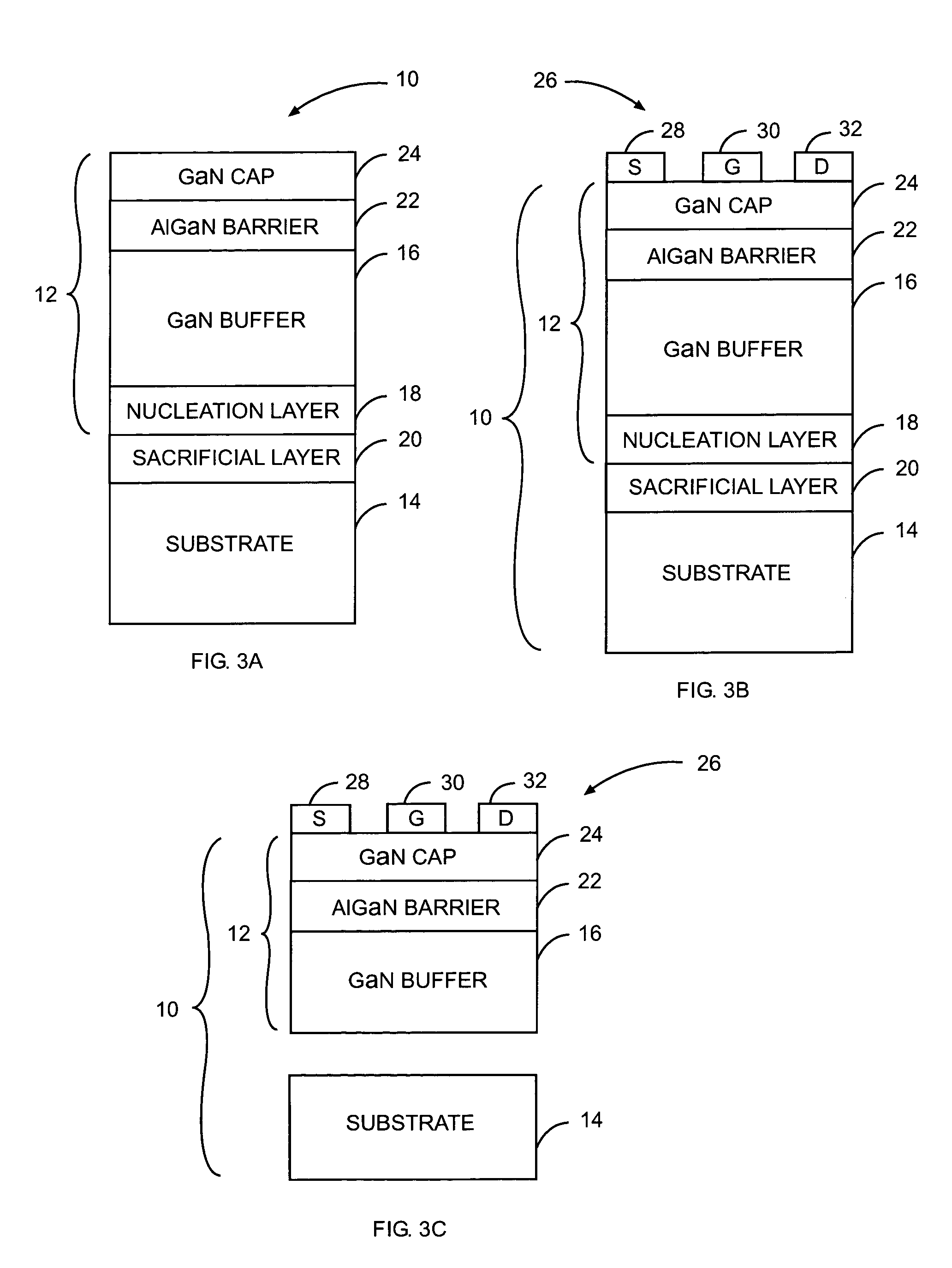
[0021]The present invention is preferably incorporated in a gallium nitride (GaN) structure 10 as illustrated in FIG. 1. In general, the present invention allows the separation of structural epitaxial layers 12 from a substrate 14. In this embodiment, the structural epitaxial layers 12 include a GaN buffer 16 and a nucleation layer 18, which are separated from the substrate 14 by oxidizing a sacrificial layer 20 and optionally the...
PUM
 Abstract
Description
Claims
Application Information
 - Generate Ideas
- Intellectual Property
- Life Sciences
- Materials
- Tech Scout
- Unparalleled Data Quality
- Higher Quality Content
- 60% Fewer Hallucinations
Browse by: Latest US Patents, China's latest patents, Technical Efficacy Thesaurus, Application Domain, Technology Topic, Popular Technical Reports.
© 2025 PatSnap. All rights reserved.Legal|Privacy policy|Modern Slavery Act Transparency Statement|Sitemap|About US| Contact US: help@patsnap.com