Methods for minimizing the impedance discontinuity between a conductive trace and a component and structures formed thereby

Inactive Publication Date: 2006-04-25
INTEL CORP
View PDF18 Cites 12 Cited by
  • Summary
  • Abstract
  • Description
  • Claims
  • Application Information

AI Technical Summary

Problems solved by technology

As chip size continues to be reduced and signals are clocked at ever increasing frequencies, high-speed, high-frequency signals being driven between chips via traces on a printed circuit boards (“PCB's”) may be subject to detrimental impedance effects.
One manifestation of these impedance effects is unwanted reflections due to impedance mismatches (i.e., impedance discontinuities between a signal trace and a component, for example, that may impair the performance and reliability of a circuit).
The high-speed, high-frequency signals may also be prone to cross-talk and electromagnetic interference (“EMI”).
Any impedance discontinuity in this area will inevitably appear as an inaccurate TDR reading.
However, this type of connector installation is usually less than satisfactory, since it may contribute to an impedance discontinuity between the probe and the circuit board at high frequencies.
However, a wide trace may use too much PCB area (real estate) in certain implementations.

Method used


Image

  • Methods for minimizing the impedance discontinuity between a conductive trace and a component and structures formed thereby
  • Methods for minimizing the impedance discontinuity between a conductive trace and a component and structures formed thereby
  • Methods for minimizing the impedance discontinuity between a conductive trace and a component and structures formed thereby

Examples


Embodiment Construction

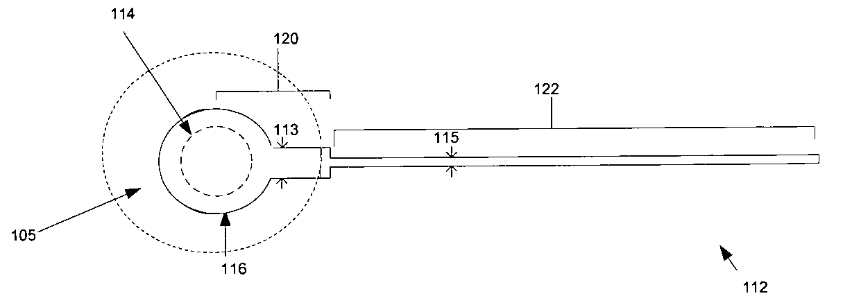
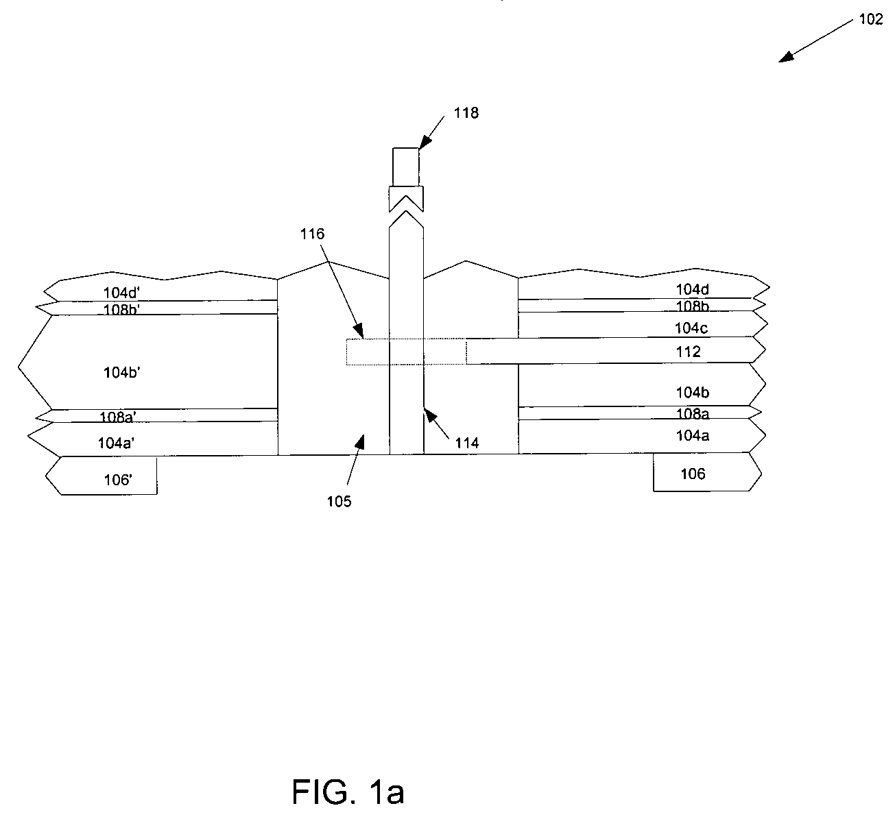
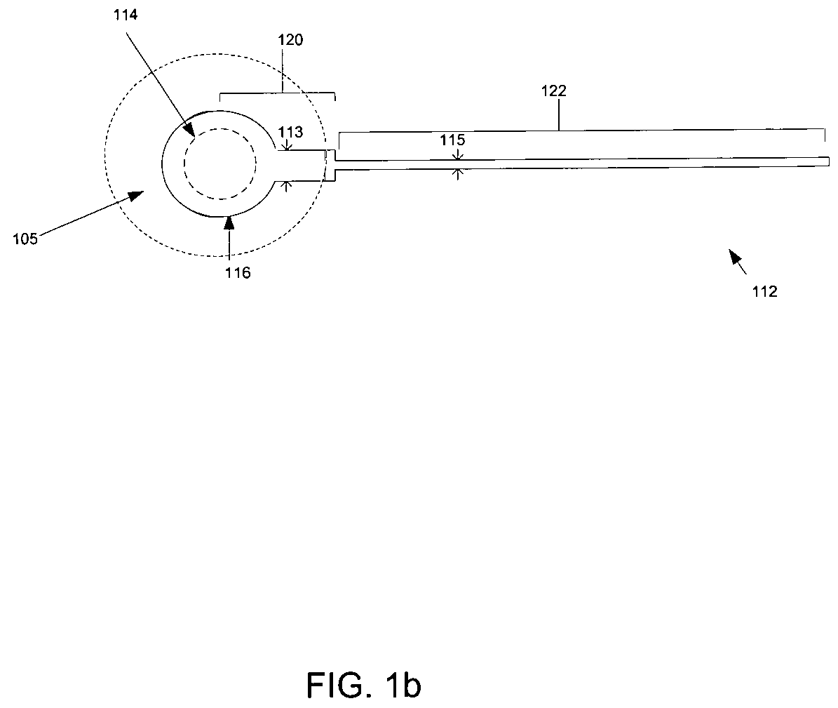
[0019]In the following detailed description, reference is made to the accompanying drawings that show, by way of illustration, specific embodiments in which the invention may be practiced. These embodiments are described in sufficient detail to enable those skilled in the art to practice the invention. It is to be understood that the various embodiments of the invention, although different, are not necessarily mutually exclusive. For example, a particular feature, structure, or characteristic described herein, in connection with one embodiment, may be implemented within other embodiments without departing from the spirit and scope of the invention. In addition, it is to be understood that the location or arrangement of individual elements within each disclosed embodiment may be modified without departing from the spirit and scope of the invention. It is further to be understood that such terms as top and bottom are relative terms that may be interchangeable depending upon the partic...


PUM


Abstract

Methods and apparatus that minimize the impedance discontinuity between a component and a signal trace is described. The methods and apparatus generally comprise at least one signal trace disposed on a dielectric layer, wherein the signal trace comprises a first width which is wider than a second width, a via connected to the first width of the signal trace, and a component electrically attached to the via, wherein an impedance discontinuity between the signal trace and the component is lowered.

Description

FIELD OF THE INVENTION[0001]The present invention relates generally to circuit boards, test structures and test systems, as well as methods to form such circuit boards, test structures and test systems, and more specifically to structures and methods for minimizing the impedance discontinuity between a conductive trace and a component.BACKGROUND OF THE INVENTION[0002]As chip size continues to be reduced and signals are clocked at ever increasing frequencies, high-speed, high-frequency signals being driven between chips via traces on a printed circuit boards (“PCB's”) may be subject to detrimental impedance effects. One manifestation of these impedance effects is unwanted reflections due to impedance mismatches (i.e., impedance discontinuities between a signal trace and a component, for example, that may impair the performance and reliability of a circuit). The high-speed, high-frequency signals may also be prone to cross-talk and electromagnetic interference (“EMI”).[0003]One way of...

Claims


Application Information

Patent Timeline
IPC IPC(8): G01R31/11H03H7/38H05K7/02G01R31/28H05K1/02H05K1/11H05K3/42
CPCG01R31/2812G01R31/2818H05K1/0251H05K1/116H05K2201/09727H05K3/429H05K2201/09454H05K2201/09718
Inventor YE, XIAONINGMILLER, DENNISBOLEN, JERRY D.
Owner INTEL CORP
Why Eureka
Try Eureka