Touch panel and electronic device

a technology of electronic devices and touch panels, applied in the field of touch panels, can solve the problems of lower light transmittance of the touch panel, and lower visibility of the display device provided with this type of touch panel, and achieve the effect of reducing light reflection and diffraction at the boundary between the air space and the transparent electrod

Inactive Publication Date: 2006-04-25
SEIKO EPSON CORP
View PDF17 Cites 58 Cited by
  • Summary
  • Abstract
  • Description
  • Claims
  • Application Information

AI Technical Summary

Benefits of technology

[0024]In the touch panel of the electronic device, the light reflection and diffraction at the boundary between the air space and the transparent electrode can be reduced.

Problems solved by technology

This leads to lower light transmittance of the touch panel, thereby possibly resulting in lower visibility of the display device.
Though the liquid space interposed between the pair of substrates prevents the light reflection at the surface of the transparent electrode, air bubbles may be formed in the liquid space, thereby possibly causing a problem of lower visibility of the display device provided with this type of touch panel.

Method used


Image

  • Touch panel and electronic device
  • Touch panel and electronic device
  • Touch panel and electronic device

Examples


first embodiment

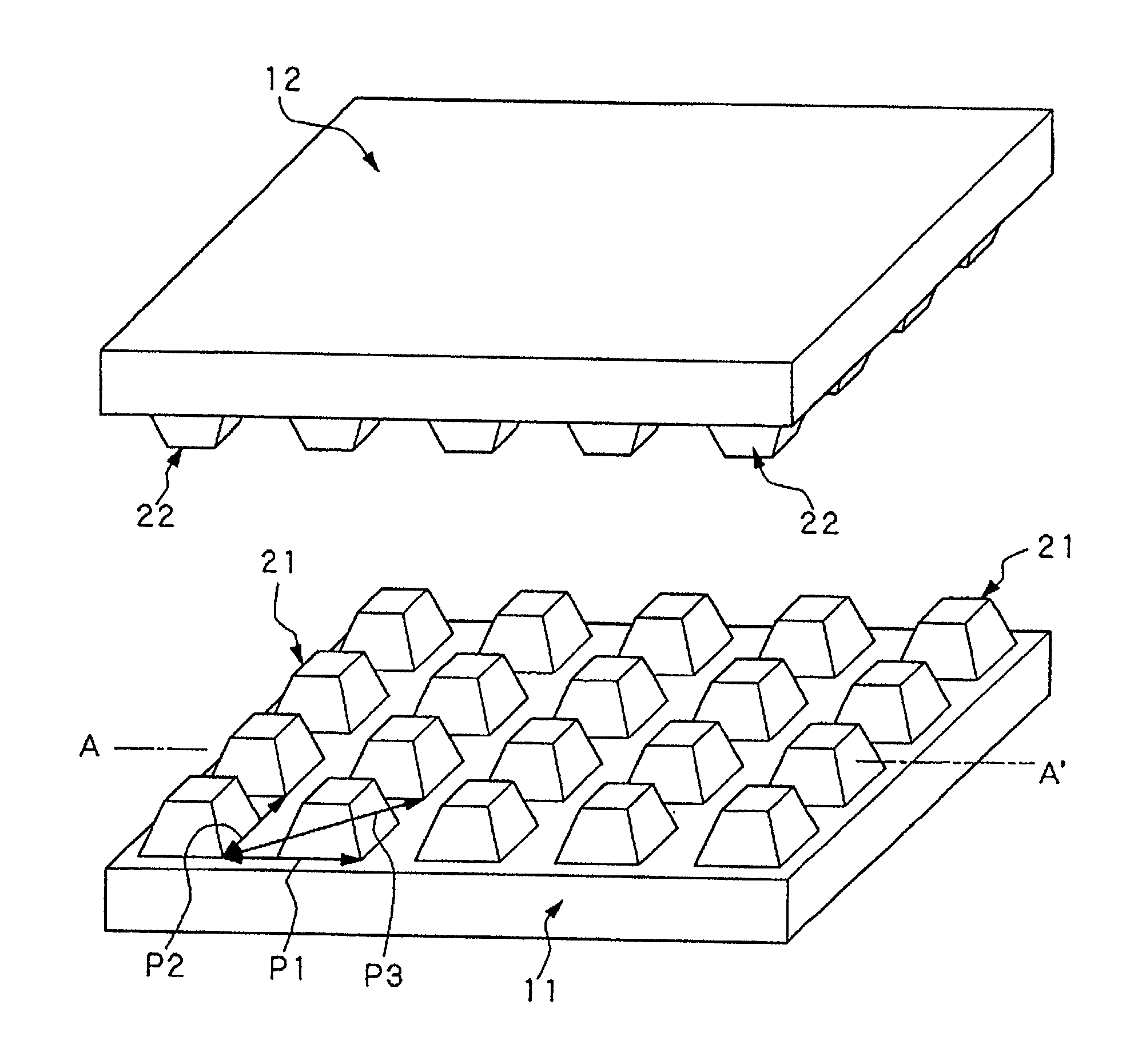
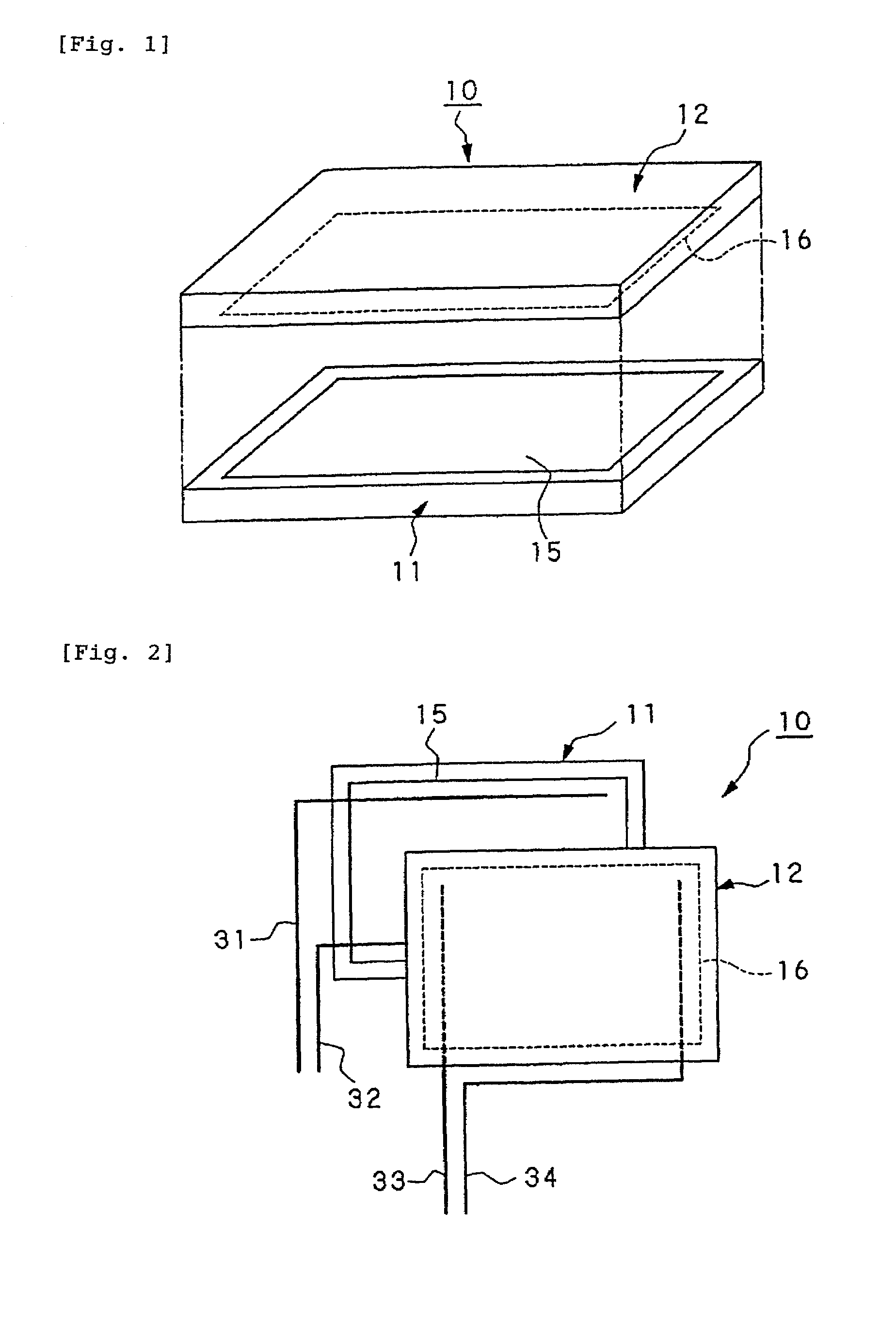
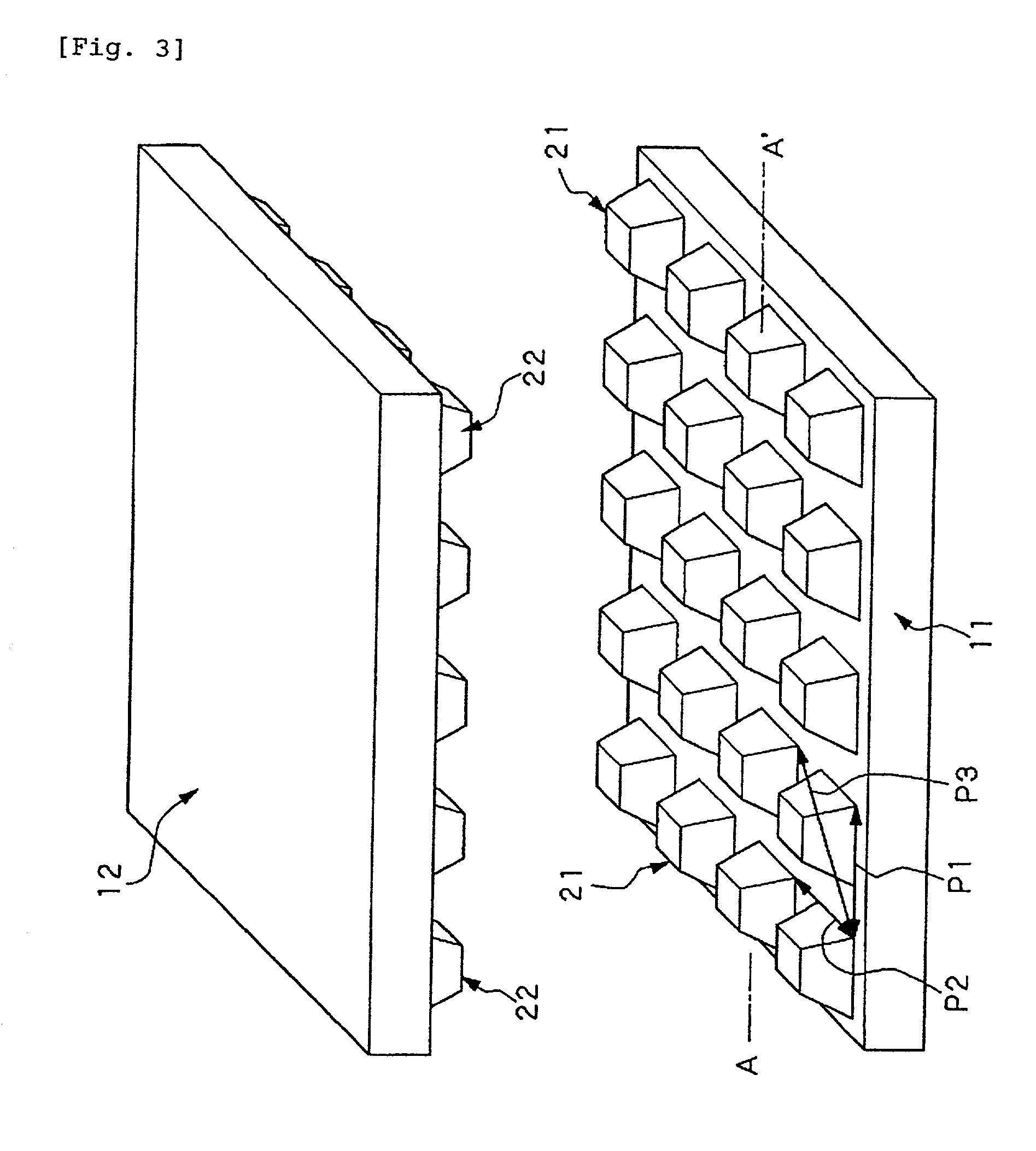
[0038]The structure of an analog resistive contact-type touch panel according to the present invention will be described with reference to FIGS. 1 to 4. FIG. 1 is an exploded perspective view of the overall structure of the touch panel according to the embodiment. FIG. 2 is a plan view of the overall structure of the touch panel according to the embodiment. FIG. 3 is a fragmentary exploded perspective view of the touch panel according to the embodiment in an enlarged scale. FIG. 4 is a fragmentary sectional view of the touch panel according to the embodiment in an enlarged scale.

[0039]FIG. 2 is a plan view wherein the touch panel is viewed from above an upper substrate of the touch panel such that a lower substrate and the upper substrate of the touch panel are staggered while being parallel to each other. FIG. 3 is a perspective view of the lower substrate and the upper substrate alone, which will be described later, of the touch panel according to the embodiment. FIG. 4 is a secti...

second embodiment

[0080]In the second embodiment, as described above, the lower transparent electrode 55 having the large number of fine projections 61 arranged with the substantially periodical pitches P4, P5, and P6 shorter than any wavelength of visible light is formed on the inner surface of the flat lower substrate 51. The same applies to the combination of the upper transparent electrode 56, the upper substrate 52, and the large number of projections 62.

[0081]Thus, projections and depressions having a predetermined shape are also formed on the inner surface of the lower transparent electrode 55 with the substantially periodical pitches P4, P5, and P6 shorter than any wavelength of visible light. The same applies to the combination of the upper transparent electrode 56 and the large number of fine projections 62. With this structure, the light reflection and diffraction at the boundary between the air space 13 and the lower transparent electrode 55 and at the boundary between the air space 13 an...

third embodiment

[0088]The analog resistive contact-type touch panel has the lower transparent electrode and the upper transparent electrode formed on substantially the entire inner surfaces of the lower substrate and the upper substrate, respectively. Meanwhile, a touch panel 70 has lower transparent electrodes 75 and upper transparent electrodes 76 formed on the inner surfaces of a lower substrate 71 and an upper substrate 72 in a stripe-like configuration, respectively. In addition, the lower transparent electrodes 75 and the upper transparent electrodes 76 are arranged so as to cross each other.

[0089]Each of the lower transparent electrodes 75 is connected to a corresponding line of wiring 81 so that the lower transparent electrode 75 has its own electric potential. The same applies to the combination of each of the upper transparent electrodes 76, a corresponding line of wiring 82, and the upper transparent electrodes 76.

[0090]The touch panel 70 according to the third embodiment is configured ...


PUM


Abstract

The present invention provides a touch panel having pluralities of projections, each of the projections having a predetermined shape, formed on inner surfaces of a lower substrate and an upper substrate, respectively. The projections being formed in at least two directions with a substantially periodical pitch that is shorter than any wavelength of visible light. The touch panel can also include a lower transparent electrode and an upper transparent electrode formed over the inner surfaces of the lower substrate and the upper substrate having the pluralities of projections, respectively. The cross-sectional area of each of the projections parallel to the outer surface of the lower substrate is configured to decrease continuously from bottom to top of the projection. The same applies to the combination of each of the projections, the bottom and a top thereof, and the upper substrate. Accordingly, this structure reduces the light reflection and diffraction at the boundary between an air space and the transparent electrode, thereby providing a resistive contact-type touch panel or a electrostatic capacitive coupling-type touch panel having high light transmittance.

Description

BACKGROUND OF THE INVENTION[0001]1. Field of Invention[0002]The present invention relates to a touch panel capable of input by a finger, a pen, or the like.[0003]2. Description of Related Art[0004]Currently, touch panels have been developed as coordinate detection devices, mounted on electronic devices, such as small portable information devices, and capable of input by a finger, a pen, or the like. Known touch panels for position detection as in the coordinate detection devices are of a resistive contact type and an electrostatic capacitive coupling type which can achieve a simple structure and a thin profile of the touch panels. The resistive contact type includes an analog resistive contact type and a digital resistive contact type. The former is capable of analog input, such as character input, and the latter is capable of on-off actions of a switch at the position of the touch panel touched by a finger, a pen, or the like.[0005]All types of touch panels, that is, the analog res...

Claims


Application Information

Patent Timeline
Patent Type & Authority Patents(United States)
IPC IPC(8): G09G5/00G06F3/045G06F3/03G06F3/041G06F3/044
CPCG06F3/045G06F3/044G06F3/0445G06F3/0446G06F3/03
Inventor SAKATA, HIDEFUMITAKEUCHI, TETSUHIKOIISAKA, HIDEHITOYOSHIDA, SHOHEI
Owner SEIKO EPSON CORP
Why Eureka
Try Eureka