Semiconductor assembly with a metal oxide layer having intermediate refractive index

a technology of metal oxide and semiconductors, applied in the field of semiconductor assemblies with metal oxide layers having intermediate refractive index, can solve the problem of prone to refractive errors at any interface between materials having different refractive indexes, and achieve the effect of reducing light reflection

Inactive Publication Date: 2012-04-05
GTAT CORPORATION
View PDF6 Cites 22 Cited by
  • Summary
  • Abstract
  • Description
  • Claims
  • Application Information

AI Technical Summary

Benefits of technology

[0004]The present invention is defined by the following claims, and nothing in this section should be taken as a limitation on those claims. In general, the invention is directed to a structure to reduce reflection of light at the light-facing surface of a photosensitive device such as a photovoltaic cell.

Problems solved by technology

Reflection is prone to occur at any interface between materials having different refractive indices.

Method used


Image

  • Semiconductor assembly with a metal oxide layer having intermediate refractive index
  • Semiconductor assembly with a metal oxide layer having intermediate refractive index
  • Semiconductor assembly with a metal oxide layer having intermediate refractive index

Examples


example

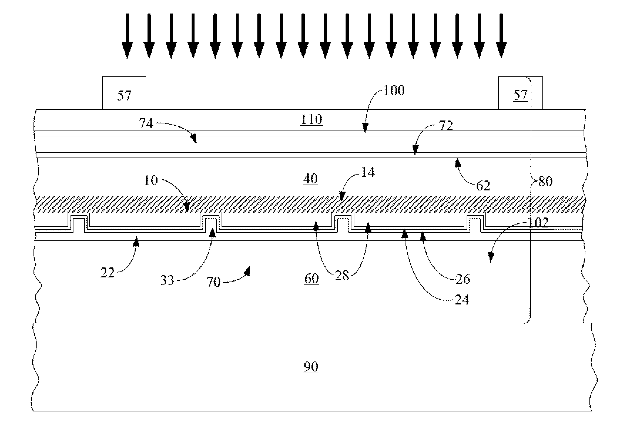
[0023]The process begins with a donor body of an appropriate semiconductor material. An appropriate donor body may be a monocrystalline silicon wafer of any practical thickness, for example from about 200 to about 1000 microns thick. Typically the wafer has a orientation, though wafers of other orientations may be used. In alternative embodiments, the donor wafer may be thicker; maximum thickness is limited only by practicalities of wafer handling. Alternatively, polycrystalline or multicrystalline silicon may be used, as may microcrystalline silicon, or wafers or ingots of other semiconductor materials, including germanium, silicon germanium, or III-V or II-VI semiconductor compounds such as GaAs, InP, etc. In this context the term multicrystalline typically refers to semiconductor material having grains that are on the order of a millimeter or larger in size, while polycrystalline semiconductor material has smaller grains, on the order of a thousand angstroms. The grains of micro...


PUM

PropertyMeasurementUnit
thicknessaaaaaaaaaa
thicknessaaaaaaaaaa
thicknessaaaaaaaaaa

Abstract

A semiconductor assembly is described with a thin metal oxide layer interposed between a transparent conductive oxide and an amorphous silicon layer, along with methods for making this structure. The metal oxide layer has a refractive index or range of refractive indices intermediate between that of the transparent conductive oxide and the amorphous silicon layer, and thus tends to reduce reflection at the interface. Such a layer can be used at the light-facing surface of a light-sensitive device such as a photovoltaic cell to maximize the amount of incident light entering the cell. Titanium oxide is a suitable metal oxide, and has a refractive index between those of silicon and of both indium tin oxide and aluminum-doped zinc oxide, two common transparent conductive oxides.

Description

BACKGROUND OF THE INVENTION[0001]The invention relates to a structure to minimize reflection at a surface of a photosensitive device.[0002]A conventional prior art photovoltaic cell includes a p-n diode; an example is shown in FIG. 1. A depletion zone forms at the p-n junction, creating an electric field. Incident photons (incident light is indicated by arrows) will knock electrons from the valence band to the conduction band, creating free electron-hole pairs. Within the electric field at the p-n junction, electrons tend to migrate toward the n region of the diode, while holes migrate toward the p region, resulting in current, called photocurrent. Typically the dopant concentration of one region will be higher than that of the other, so the junction is either a p+ / n− junction (as shown in FIG. 1) or a n+ / p− junction. The more lightly doped region is known as the base of the photovoltaic cell, while the more heavily doped region, of opposite conductivity type, is known as the emitte...

Claims


Application Information

Patent Timeline
Patent Type & Authority Applications(United States)
IPC IPC(8): H01L31/0224H01L31/18
CPCH01L31/02168H01L31/075H01L31/1804H01L31/056Y02E10/52Y02E10/548Y02E10/547H01L31/1892Y02P70/50
Inventor LIANG, KATHY J.PRABHU, GOPALAKRISHNALE, HIENMINH HUU
Owner GTAT CORPORATION
Why Eureka
Try Eureka