Photoelectric device

a photoelectric device and lens layer technology, applied in the direction of photoelectric discharge tubes, electric discharge lamps, instruments, etc., can solve the problems of reducing the light emission efficiency limiting the miniaturization of the substrate, and increasing the cost of the photoelectric device-part, so as to improve the bonding force between the lens layer and the sealing resin layer.

Inactive Publication Date: 2006-05-02
MATSUSHITA ELECTRIC WORKS LTD
View PDF5 Cites 52 Cited by
  • Summary
  • Abstract
  • Description
  • Claims
  • Application Information

AI Technical Summary

Benefits of technology

[0010]The present invention was made to solve the above problems and it is an object of the present invention to provide a photoelectric device-part in which a bonding pad can be provided without increasing a plane area occupied by a concave part for housing a photoelectric device on a substrate and its miniaturization and light usability efficiency are improved.

Problems solved by technology

However, according to the photoelectric device-part shown in FIG. 17A or disclosed in the patent document 1, since a space for a pad of a wire bonding is needed at the bottom surface of the case 110 having the centroclinal inner surface, there is a limit of miniaturization of the substrate.
In addition, according to the photoelectric device-part shown in FIG. 17B or disclosed in the patent document 2, since the bonding wire 209 is long, it becomes an obstacle in a light path, which lowers light emitting efficiency in the photoelectric device-part.
Besides, in a case where the bonding wire is formed of Au wire, if the wire is long, the costs are increased.
In addition, when the projection 303 is provided, a sectional area of the concave part 302 becomes large, which damages light converging property (usability efficiency).

Method used


Image

  • Photoelectric device
  • Photoelectric device
  • Photoelectric device

Examples


Embodiment Construction

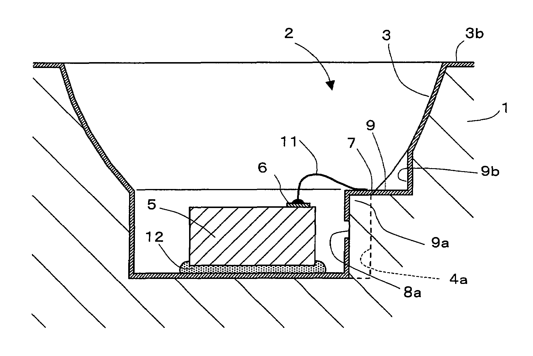
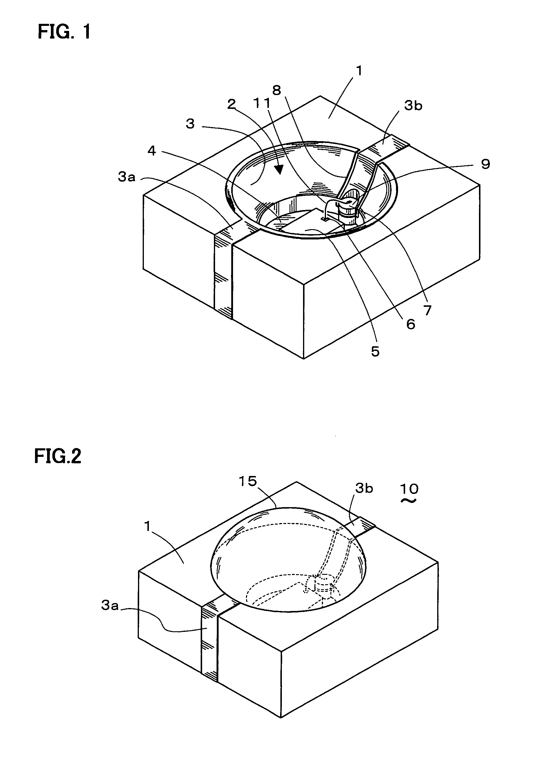
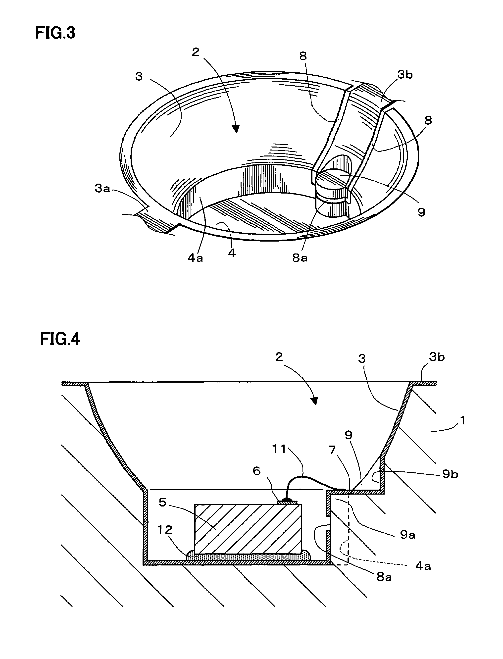
[0071]Hereinafter, a photoelectric device-part according to an embodiment of the present invention will be described with reference to accompanied drawings. FIG. 1 shows a state in which a sealing resin layer of the photoelectric device-part is excluded and FIG. 2 is an external view showing the photoelectric device-part. A photoelectric device-part 10 is formed by mounting a photoelectric device 5 on a bottom surface 4 of a concave part 2 formed in a quadrangular circuit substrate 1, which is used as a light emitting or receiving device such as a photo connector. A light axis is defined in almost a center of a light emitting or receiving she of the photoelectric device 5 in the vertical direction. A metalized light reflecting surface 3 provided for light emission or reception by the photoelectric device 5 is formed on inner surface including a slanting curved surface which forms the concave part 2.

[0072]This light reflecting surface 3 is formed by providing the slanting curved surf...


PUM


Abstract

In a photoelectric device-part, a bonding pad is formed without increasing a plane area of a concave part for housing a photoelectric device to implement miniaturization and improvement of the light usability efficiency. A light reflecting surface 3 of nearly a parabola configuration or the like provided for light emission and reception by a photoelectric device 5 is formed on a slanting curved surface constituting a concave part 2 of a circuit substrate 1. A convex portion 9a projecting from the light reflecting surface 3 and a receding concave portion 9b are formed in the middle of the concave part 2. A stage 9 is formed by an upper and bottom surfaces of the convex and concave portions 9a and 9b, respectively. A bonding pad 7 for connecting circuits of the photoelectric device 5 is formed at the stage 9. Since a space for the bonding pad 7 is provided by both concave and convex portions, deformation of the light reflecting surface 3 caused by the receding concave portion 9b and a ratio of intrusion to the bottom surface of the concave part by the projecting convex portion 9a can be both minimized. As a result, the photoelectric device 5 can be mounted without largely lowering light emission efficiency or without decentering the light emitting and receiving center, whereby a photoelectric device-part 10 can be miniaturized.

Description

BACKGROUND OF THE INVENTION[0001]1. Field of the Invention[0002]The present invention relates to a photoelectric device-part in which a photoelectric device is mounted on a concave part provided in a three-dimensional circuit substrate[0003]2. Description of the Prior Art[0004]Conventionally, a part which emits or receives light using a photoelectric device to convert light into electricity and vice versa is known as a photoelectric device-part. For example, a light emitting device 100 shown in FIG. 17A is a photoelectric device-part in which electrodes 105 and 106 are formed on a substrate 101, an LED (light emitting diode) chip 108 is mounted on the electrode 106 through an electroconductive bonding material 107 to electrically connect a lower surface of the LED chip 108 to the electrode 106, an upper electrode of the LED chip 108 is electrically connected to the electrode 105 by a wire bonding, and the LED chip on the substrate is covered with a case 110 having a centroclinal inn...

Claims


Application Information

Patent Timeline
Patent Type & Authority Patents(United States)
IPC IPC(8): H01L33/00H01L31/0203H01L31/0232H01L33/48H01L33/62
CPCH01L31/0203H01L31/0232H01L33/62H01L24/45H01L2924/30107H01L2924/12041H01L2224/45144H01L2924/1815H01L2924/01019H01L2224/73265H01L2224/48465H01L33/486H01L33/60H01L2224/48091H01L2924/00014H01L2924/00H01L2924/12042H01L2924/12043H01L2924/14H01L2924/181H01L31/02325H01L2924/00012
Inventor KIDA, SHINOBUTATSUTA, JUNYOSHIDA, HIROYUKIMASUI, MIKIO
Owner MATSUSHITA ELECTRIC WORKS LTD
Why Eureka
Try Eureka